C8051F39x/37x
14. Comparator0
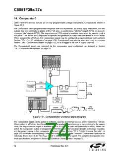
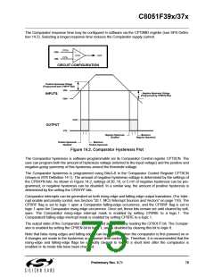
C8051F39x/37x devices include an on-chip programmable voltage comparator, Comparator0, shown in
Figure 14.1.
The Comparator offers programmable response time and hysteresis, an analog input multiplexer, and two
outputs that are optionally available at the Port pins: a synchronous “latched” output (CP0), or an asyn-
chronous “raw” output (CP0A). The asynchronous CP0A signal is available even when the system clock is
not active. This allows the Comparator to operate and generate an output with the device in STOP mode.
When assigned to a Port pin, the Comparator output may be configured as open drain or push-pull (see
Section “27.4. Port I/O Initialization” on page 178). Comparator0 may also be used as a reset source (see
Section “24.5. Comparator0 Reset” on page 157), or as a trigger to kill a PCA output channel.
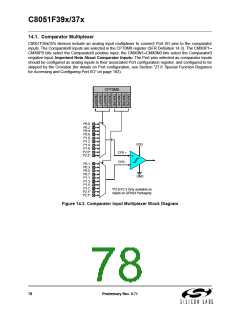
The Comparator0 inputs are selected by the comparator input multiplexer, as detailed in Section
“14.1. Comparator Multiplexer” on page 78.
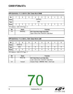
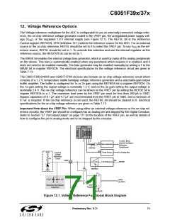
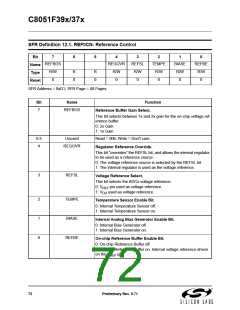
CPT0CN
VDD
CP0 +
+
CP0
Comparator
Input Mux
SET
CLR
SET
CLR
D
Q
Q
D
Q
Q
CP0 -
-
Crossbar
(SYNCHRONIZER)
CP0A
GND
Reset
Decision
Tree
CPT0MD
0
1
CP0
Interrupt
CP0EN
EA
CP0RIF
CP0FIF
0
0
1
1
0
1
Figure 14.1. Comparator0 Functional Block Diagram
The Comparator output can be polled in software, used as an interrupt source, and/or routed to a Port pin.
When routed to a Port pin, the Comparator output is available asynchronous or synchronous to the system
clock; the asynchronous output is available even in STOP mode (with no system clock active). When dis-
abled, the Comparator output (if assigned to a Port I/O pin via the Crossbar) defaults to the logic low state,
and the power supply to the comparator is turned off. See Section “27.3. Priority Crossbar Decoder” on
page 176 for details on configuring Comparator outputs via the digital Crossbar. Comparator inputs can be
externally driven from –0.25 V to (V ) + 0.25 V without damage or upset. The complete Comparator elec-
DD
trical specifications are given in Section “7. Electrical Characteristics” on page 32.
74
Preliminary Rev. 0.71

 SILICON [ SILICON ]