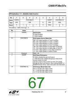
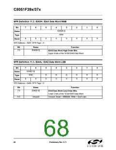
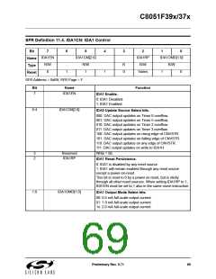
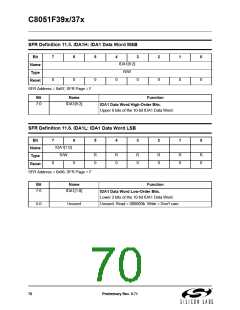
C8051F39x/37x
12. Voltage Reference Options
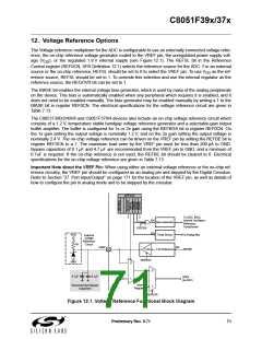
The Voltage reference multiplexer for the ADC is configurable to use an externally connected voltage refer-
ence, the on-chip reference voltage generator routed to the VREF pin, the unregulated power supply volt-
age (V ), or the regulated 1.8 V internal supply (see Figure 12.1). The REFSL bit in the Reference
DD
Control register (REF0CN, SFR Definition 12.1) selects the reference source for the ADC. For an external
source or the on-chip reference, REFSL should be set to 0 to select the VREF pin. To use V as the ref-
DD
erence source, REFSL should be set to 1. To override this selection and use the internal regulator as the
reference source, the REGOVR bit can be set to 1.
The BIASE bit enables the internal voltage bias generator, which is used by many of the analog peripherals
on the device. This bias is automatically enabled when any peripheral which requires it is enabled, and it
does not need to be enabled manually. The bias generator may be enabled manually by writing a 1 to the
BIASE bit in register REF0CN. The electrical specifications for the voltage reference circuit are given in
Table 7.13.
The C8051F390/2/4/6/8 and C8051F370/4 devices also include an on-chip voltage reference circuit which
consists of a 1.2 V, temperature stable bandgap voltage reference generator and a selectable-gain output
buffer amplifier. The buffer is configured for 1x or 2x gain using the REFBGS bit in register REF0CN. On
the 1x gain setting the output voltage is nominally 1.2 V, and on the 2x gain setting the output voltage is
nominally 2.4 V. The on-chip voltage reference can be driven on the VREF pin by setting the REFBE bit in
register REF0CN to a 1. The maximum load seen by the VREF pin must be less than 200 µA to GND.
Bypass capacitors of 0.1 µF and 4.7 µF are recommended from the VREF pin to GND, and a minimum of
0.1uF is required. If the on-chip reference is not used, the REFBE bit should be cleared to 0. Electrical
specifications for the on-chip voltage reference are given in Table 7.13.
Important Note about the VREF Pin: When using either an external voltage reference or the on-chip ref-
erence circuitry, the VREF pin should be configured as an analog pin and skipped by the Digital Crossbar.
Refer to Section “27. Port Input/Output” on page 171 for the location of the VREF pin, as well as details of
how to configure the pin in analog mode and to be skipped by the crossbar.
REF0CN
To ADC, IDAC,
Internal Oscillators,
Reference,
TempSensor
EN
EN
Bias Generator
Temp Sensor
IOSCEN
VDD
To Analog Mux
REFBE
External
Voltage
Reference
Circuit
R1
VREF
EN
1x/2x
1.2V Reference
REFBGS
GND
0
1
0
1
+
4.7F
0.1F
VREF
(to ADC)
VDD
Internal
Regulator
Recommended Bypass
Capacitors
REGOVR
Figure 12.1. Voltage Reference Functional Block Diagram
Preliminary Rev. 0.71
71

 SILICON [ SILICON ]