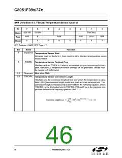
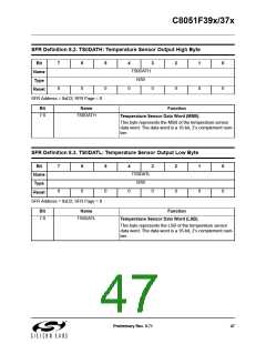
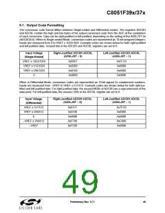
C8051F39x/37x
9.2. Modes of Operation
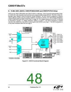
ADC0 has a maximum conversion speed of 500 ksps. The ADC0 conversion clock is a divided version of
the system clock, determined by the AD0SC bits in the ADC0CF register.
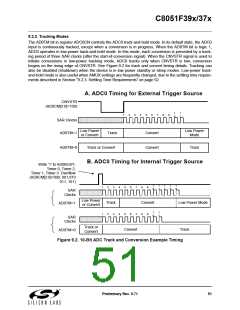
9.2.1. Starting a Conversion
A conversion can be initiated in one of several ways, depending on the programmed states of the ADC0
Start of Conversion Mode bits (AD0CM2–0) in register ADC0CN. Conversions may be initiated by one of
the following:
1. Writing a 1 to the AD0BUSY bit of register ADC0CN
2. A Timer 0 overflow (i.e., timed continuous conversions)
3. A Timer 2 overflow
4. A Timer 1 overflow
5. A rising edge on the CNVSTR input signal
6. A Timer 3 overflow
7. A Timer 4 overflow
8. A Timer 5 overflow
Writing a 1 to AD0BUSY provides software control of ADC0 whereby conversions are performed "on-
demand". During conversion, the AD0BUSY bit is set to logic 1 and reset to logic 0 when the conversion is
complete. The falling edge of AD0BUSY triggers an interrupt (when enabled) and sets the ADC0 interrupt
flag (AD0INT). Note: When polling for ADC conversion completions, the ADC0 interrupt flag (AD0INT)
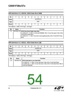
should be used. Converted data is available in the ADC0 data registers, ADC0H:ADC0L, when bit AD0INT
is logic 1. Note that when Timer 2, 3, 4, or 5 overflows are used as the conversion source, Low Byte over-
flows are used if the timer is in 8-bit mode; High byte overflows are used if the timer is in 16-bit mode. See
Section “31. Timers” on page 240 for timer configuration.
Important Note About Using CNVSTR: The CNVSTR input pin also functions as a Port I/O pin. When the
CNVSTR input is used as the ADC0 conversion source, the associated pin should be skipped by the Digi-
tal Crossbar. See Section “27. Port Input/Output” on page 171 for details on Port I/O configuration.
50
Preliminary Rev. 0.71

 SILICON [ SILICON ]