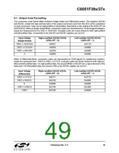
C8051F39x/37x
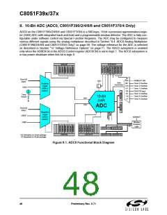
9. 10-Bit ADC (ADC0, C8051F390/2/4/6/8 and C8051F370/4 Only)
ADC0 on the C8051F390/2/4/6/8 and C8051F370/4 is a 500 ksps, 10-bit successive-approximation-regis-
ter (SAR) ADC with integrated track-and-hold and a programmable window detector. The ADC is fully con-
figurable under software control via Special Function Registers. The ADC may be configured to measure
various different signals using the analog multiplexer described in Section “9.4. ADC0 Analog Multiplexer
(C8051F390/2/4/6/8 and C8051F370/4 Only)” on page 59. The voltage reference for the ADC is selected
as described in Section “12. Voltage Reference Options” on page 71. The ADC0 subsystem is enabled
only when the AD0EN bit in the ADC0 Control register (ADC0CN) is set to logic 1. The ADC0 subsystem is
in low power shutdown when this bit is logic 0.
AMX0P
ADC0CN
Port I/O
Pins*
000
001
010
011
100
101
110
111
AD0BUSY (W)
VDD
Start
Conversion
Timer 0 Overflow
Timer 2 Overflow
Timer 1 Overflow
CNVSTR Input
Positive
Input
(AIN+)
AMUX
VDD
Timer 3 Overflow
Timer 4 Overflow
Timer 5 Overflow
Temp
Sensor
10-Bit
SAR
AIN+
AIN-
ADC
Port I/O
Pins*
Negative
Input
(AIN-)
VREF
GND
AD0WINT
AMUX
Window
Compare
Logic
32
ADC0LTH ADC0LTL
ADC0GTH ADC0GTL
AMX0N
ADC0CF
* 20 Selections on 24-pin package
16 Selections on 20-pin package
Figure 9.1. ADC0 Functional Block Diagram
48
Preliminary Rev. 0.71

 SILICON [ SILICON ]