C8051F39x/37x
9.1. Output Code Formatting
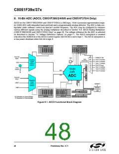
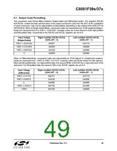
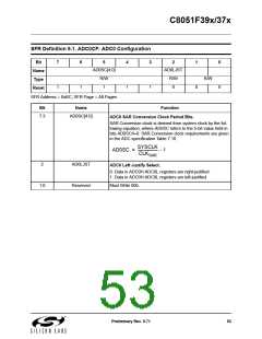
The conversion code format differs between Single-ended and Differential modes. The registers ADC0H
and ADC0L contain the high and low bytes of the output conversion code from the ADC at the completion
of each conversion. Data can be right-justified or left-justified, depending on the setting of the AD0LJST bit
(ADC0CN.0). When in Single-ended Mode, conversion codes are represented as 10-bit unsigned integers.
Inputs are measured from 0 to VREF x 1023/1024. Example codes are shown below for both right-justified
and left-justified data. Unused bits in the ADC0H and ADC0L registers are set to 0.
Input Voltage
Right-Justified ADC0H:ADC0L
Left-Justified ADC0H:ADC0L
(AD0LJST = 0)
(AD0LJST = 1)
(Single-Ended)
VREF x 1023/1024
VREF x 512/1024
VREF x 256/1024
0
0x03FF
0x0200
0x0100
0x0000
0xFFC0
0x8000
0x4000
0x0000
When in Differential Mode, conversion codes are represented as 10-bit signed 2s complement numbers.
Inputs are measured from –VREF to VREF x 511/512. Example codes are shown below for both right-jus-
tified and left-justified data. For right-justified data, the unused MSBs of ADC0H are a sign-extension of the
data word. For left-justified data, the unused LSBs in the ADC0L register are set to 0.
Input Voltage
(Differential)
Right-Justified ADC0H:ADC0L
Left-Justified ADC0H:ADC0L
(AD0LJST = 0)
(AD0LJST = 1)
VREF x 511/512
VREF x 256/512
0
0x01FF
0x0100
0x0000
0xFF00
0xFE00
0x7FC0
0x4000
0x0000
0xC000
0x8000
–VREF x 256/512
–VREF
Preliminary Rev. 0.71
49

 SILICON [ SILICON ]