GP1A52HRJ00F
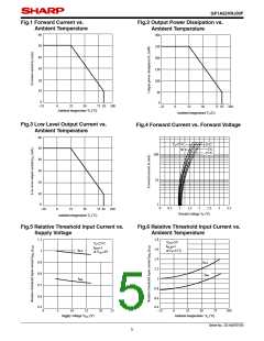
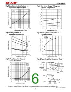
Fig.7 Low Level Output Voltage vs.
Low Level Output Current
Fig.8 Low Level Output Voltage vs.
Ambient Temperature
0.6
1
VCC=5V
VCC=5V
Ta=25˚C
0.5
0.4
0.3
0.2
0.1
0
I
OL=30mA
0.1
16mA
5mA
0.01
1
2
5
10
20
50
100
−25
0
25
50
75
100
Low level output current IOL (mA)
Ambient temperature Ta (˚C)
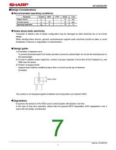
Fig.9 Supply Current vs.
Fig.10 Propagation Delay Time vs.
Forward Current
Ambient Temperature
12
3
VCC=5V
RL=280Ω
Ta=25˚C
tPHL
10
8
VCC=17V
2
1
10V
5V
ICCL
6
4
VCC=17V
tPLH
ICCH
2
0
10V
5V
0
−25
0
25
50
75
100
0
10
20
30
40
50
60
Ambient temperature Ta (˚C)
Forward current IF (mA)
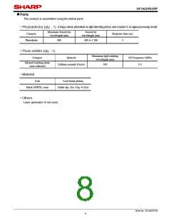
Fig.11 Rise Time,Fall Time vs.
Fig.12 Test Circuit for Response Time
Load Resistance
0.8
Voltage regulator
IF=5mA
Input
+5V
Ta=25˚C
VCC=5V
IF=5mA
0.7
0.6
0.5
0.4
0.3
0.2
280Ω
Output
(15kΩ)
tr=tf=0.01μs
ZO=50Ω
0.01μF
47Ω
Amp.
tr
GND
Input
50%
tPLH
tPHL
0.1
0
tf
VOH
90%
1.5V
Output
10%
0.1
1
10
VOL
Load resistance RL (kΩ)
tr
tf
Remarks : Please be aware that all data in the graph are just for reference and not for guarantee.
Sheet No.: D3-A03701EN
6

 SHARP [ SHARP ELECTRIONIC COMPONENTS ]