SX1232
WIRELESS & SENSING
DATASHEET
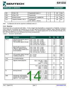
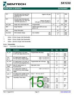
IIP2
IIP3
2nd order Input Intercept Point
Unwanted tones are 20 MHz
above the LO
-
+57
-
dBm
Highest LNA gain
3rd order Input Intercept point
Unwanted tones are 1MHz and
1.995 MHz above the LO
-
-
-12
-8
-
-
dBm
dBm
Highest LNA gain G1
LNA gain G2, 4dB sensitivity hit
BW_SSB
IMR
Single Side channel filter BW
Image Rejection
Programmable
2.7
-
-
250
-
kHz
dB
Wanted signal 3dB over sens
BER=0.1%
48
IMA
Image Attenuation
-
56
-
dB
DR_RSSI
RSSI Dynamic Range
AGC enabled
Min
Max
-
-
-127
0
-
-
dBm
dBm
*
RxBw = 83 kHz (Single Side Bandwidth)
RxBw = 50 kHz (Single Side Bandwidth)
RxBw = 250 kHz (Single Side Bandwidth)
**
***
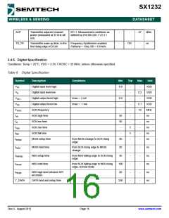
2.4.4. Transmitter
Table 7 Transmitter Specification
Symbol
Description
Conditions
Min
Typ
Max
Unit
RF_OP
RF output power in 50 ohms
Programmable with steps
on RFO pin (High efficiency PA).
Max
Min
+11
-
+14
-1
-
-
dBm
dBm
RF output power stability on
RFO pin versus voltage supply.
VDD = 2.5 V to 3.3 V
VDD = 1.8 V to 3.7 V
-
-
3
8
-
-
dB
dB
ΔRF_
OP_V
RF_OPH
RF output power in 50 ohms, on
PA_BOOST pin (Regulated PA).
Programmable with 1dB steps Max
Min
-
-
+17
+2
-
-
dBm
dBm
RF_OPH
_MAX
Max RF output power, on
PA_BOOST pin
High power mode
-
+20
-
dBm
RF output power stability on
PA_BOOST pin versus voltage
supply.
VDD = 2.4 V to 3.7 V
-
±1
-
dB
ΔRF_
OPH_V
RF output power stability versus
temperature on both RF pins.
From T = -40 °C to +85 °C
-
+/-1
-
dB
ΔRF_T
PHN
Transmitter Phase Noise
Low Consumption PLL, 915 MHz
50kHz Offset
-
-
-
-102
-114
-120
-
-
-
dBc/
Hz
400kHz Offset
1MHz Offset
Low Phase Noise PLL, 915 MHz
50kHz Offset
-
-
-
-106
-117
-122
-
-
-
dBc/
Hz
400kHz Offset
1MHz Offset
Rev 3 - August 2012
Page 15
www.semtech.com

 SEMTECH [ SEMTECH CORPORATION ]