SX1232
WIRELESS & SENSING
DATASHEET
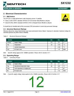
2. Electrical Characteristics
2.1. ESD Notice
The SX1232 is a high performance radio frequency device. It satisfies:
Class 2 of the JEDEC standard JESD22-A114-B (Human Body Model) on all pins.
Class III of the JEDEC standard JESD22-C101C (Charged Device Model) on all pins
It should thus be handled with all the necessary ESD precautions to avoid any permanent damage.
2.2. Absolute Maximum Ratings
Stresses above the values listed below may cause permanent device failure. Exposure to absolute maximum ratings for
extended periods may affect device reliability.
Table 2 Absolute Maximum Ratings
Symbol
Description
Min
Max
Unit
VDDmr
Tmr
Tj
Supply Voltage
Temperature
-0.5
3.9
+115
+125
+10
V
-55
° C
Junction temperature
RF Input Level
-
-
° C
Pmr
dBm
Note Specific ratings apply to the +20dBm operation. Please refer to Section 3.4.7.
2.3. Operating Range
Table 3 Operating Range
Symbol
Description
Min
Max
Unit
VDDop
Top
Supply voltage
1.8
-40
-
3.7
+85
25
V
Operational temperature range
Load capacitance on digital ports
RF Input Level
°C
Clop
ML
pF
dBm
-
+10
Note A specific supply voltage range applies to the +20dBm operation. Please refer to Section 3.4.7.
Rev 3 - August 2012
Page 12
www.semtech.com

 SEMTECH [ SEMTECH CORPORATION ]