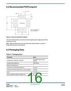
6.2 Recommended PCB Footprint
0.35
0.65
0.55
3.70
2.76
CENTER PAD
NOTE: All dimensions
are in millimeters.
2.76
3.70
Figure 6-2: Recommended PCB Footprint
The Center Pad should be connected to the most negative power supply plane (VEE) by
a minimum of 5 vias.
Note: Suggested dimensions only. Final dimensions should conform to customer
design rules and process optimizations.
6.3 Packaging Data
Table 6-1: Packaging Data
Parameter
Value
16-pin QFN / 4mm x 4mm /
0.65mm
Package type / dimensions / pad pitch
Package Drawing Reference
JEDEC M0220
3
Moisture Sensitivity Level
Junction to Case Thermal Resistance, θj-c
31.0°C/W
Junction to Air Thermal Resistance, θj-a (at zero airflow)
43.8°C/W
11.0°C/W
Yes
Psi, Ψ
Pb-free and RoHS compliant, Halogen-free
GS2988
Final Data Sheet
16 of 18
Semtech
www.semtech.com
Rev.6
GENDOC-052131 July 2015

 SEMTECH [ SEMTECH CORPORATION ]