5. Application Information
5.1 PCB Layout
Special attention must be paid to component layout when designing serial digital
interfaces for HDTV.
An FR-4 dielectric can be used, however, controlled impedance transmission lines are
required for PCB traces longer than approximately 1cm. Note the following PCB artwork
features used to optimize performance:
•
The PCB trace width for HD rate signals is closely matched to SMT component
width to minimize reflections due to changes in trace impedance
•
The PCB ground plane is removed under the GS2988 output components to
minimize parasitic capacitance (Note: care should be taken, as removing too much
of the plane will make the system susceptible to EMI)
•
The PCB ground plane is removed under the GS2988 RSET pin and resistor to
minimize parasitic capacitance. The RSET resistor should be directly connected to
the VCC plane
•
•
Input and output BNC connectors are surface mounted in-line to eliminate a
transmission line stub caused by a BNC mounting via high-speed traces
High-speed traces are curved to minimize impedance variations due to change of
PCB trace width
Note: For more recommendations on Trace Lengths, ORL Inductor Values and other PCB
Layout Considerations, please refer to Semtech’s GS2989 Design Guide
(Doc ID 52070).
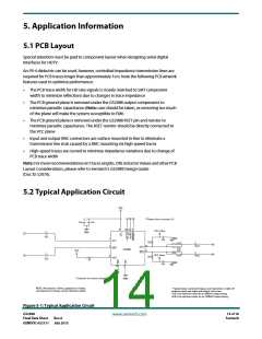
5.2 Typical Application Circuit
VCC
**Please refer to section 4.2.
10n
10n
9
16 10
6
VCC_Term
10n
GND
4u7
4u7
GND
5n6*
1
2
DDI
DDI
75R
75R
12
11
4u7
4u7
SDO
SDO
75R
75R
GS2988
VCC
VCC_Term
10n
5n6*
4
RSET
R*
GND
14
3
*Customer to choose resistor value.
GND
NOTE: All resistors in Ohms, capacitors in Farads,
and inductors in Henrys, unless otherwise stated.
* Typical value: varies with layout, and represents a trade-off
between good eye shape and output return loss.
5n6 is the optimum value for an 800mV output swing.
6n8 is the optimum value for an 1800mV output swing.
Figure 5-1: Typical Application Circuit
GS2988
Final Data Sheet
14 of 18
Semtech
www.semtech.com
Rev.6
GENDOC-052131 July 2015

 SEMTECH [ SEMTECH CORPORATION ]