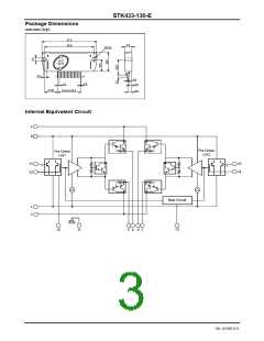
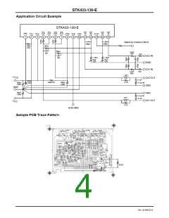
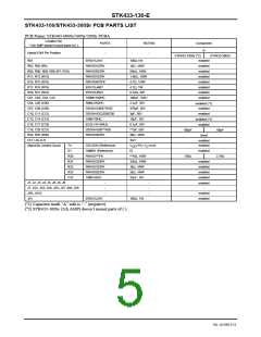
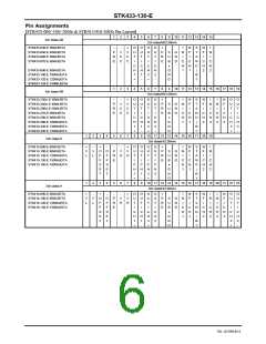
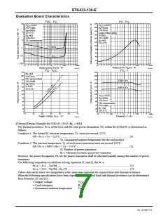
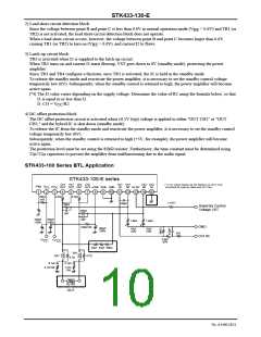
STK433-130-E
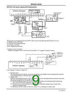
STK433-100 Series Application Explanation
Stand-by Circuit
in Pre Driver IC
SW transistor
STK433-100 series
ΔV
BE
1) Stand-by control circuit part
H: Operation mode (+5V)
L: Stand-by mode (0V)
Ch1
Ch1
Ch2
Ch2
Ch1 Ch1
Ch2
NF
Ch2
IN
-PRE -V
1
+V
+PRE
8
GND
SUB
9
IN
NF
ST-BY
CC
OUT(+)
OUT(-) OUT(+)
OUT(-)
CC
2
3
4
6
7
10
11
12
13
14
15
1kΩ
5
6.8kΩ
6.8kΩ
56kΩ
33kΩ
56kΩ
(*1) R1
Stand-By Control
Tr5
Voltage VST
IST
13kΩ
2kΩ
33μF
Tr1
Tr2
Point.B
Point.B
Point.C
I2
Point.C
22kΩ
56kΩ
(2) Load short
detection part
I3
Tr4
(*4) R2
1kΩ
0.1μF
10kΩ
Tr3
(3) Latch-up
circuit part
100kΩ
-V
CC
Tr5
82kΩ
Tr6
OUT Ch1
OUT Ch2
22μF
82kΩ 22μF
100
kΩ
(4) DC offset
protection
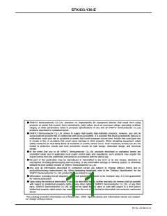
The protection circuit application for the STK433-100sr consists of the following blocks (blocks (1) to (4)).
(1) Standby control circuit block
(2) Load short-circuit detection block
(3) Latch-up circuit block
(4) DC voltage protection block
1) Standby control circuit block
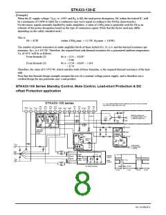
(Reference example) STK433-100 series test circuit (when +5V is applied to Stand-by control.)
1) Stand-by control
1kΩ (*3)
H: Operation mode (+5V)
L: Stand-by mode (0V)
33kΩ
(*1) R1
Stand-By Control
Voltage VST
13kΩ
33μF
(*2)
2kΩ (*3)
ΔVBE
Sink current IST
1
2
3
4
6
7
8
9
10
11
12
13
14
15
5
ex) Stand-by control voltage=+5V
IST=(VST-VBE*2)/R1
=(5-0.6*2)/13kΩ
-PRE -V
+V
Ch1
Ch1
Ch2
Ch2
Ch1 Ch1
Ch2
NF
Ch2
IN
+PRE
GND
ST-BY
CC
SUB
CC
OUT
OUT
OUT
OUT
IN
NF
≈0.3(mA)
ΔVBE
Stand-by Circuit
in Pre Driver IC
STK433-100series
Concerning pin 13 reference voltage VST
<1> Operation mode
The switching transistor in the bias circuit turns on and places the amplifier into the operating mode when the
current flowing into pin 13 (IST) becomes 0.25mA or greater.
<2> Standby mode
When the current flowing into pin 13 (IST) is stopped (=0mA), the switching transistor in the bias circuit turns
off, placing the amplifier into the standby mode.
(*1) The current limiting resistor (R1) must be used to ensure that the current flowing into the stand-by pin
(pin 13) does not exceed its maximum rated value IST max.
(*2) The pop noise level when the power is turned on can be reduced by setting the time constant with a
capacitor in operating mode.
(*3) Determines the time constant at which the capacitor (*2) is discharged in standby mode.
No. A1596-9/11

 SANYO [ SANYO SEMICON DEVICE ]