STK433-130-E
[Example]
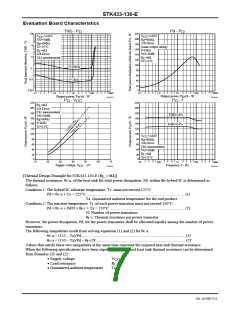
When the IC supply voltage, V , is 44V and R is 6Ω, the total power dissipation, Pd, within the hybrid IC, will
CC
L
be a maximum of 130W at 1kHz for a continuous sine wave signal according to the Pd-P characteristics.
O
For the music signals normally handled by audio amplifiers, a value of 1/8P max is generally used for Pd as an
O
estimate of the power dissipation based on the type of continuous signal. (Note that the factor used may differ
depending on the safety standard used.)
This is:
Pd ≈ 87W
(when 1/8P max. = 12.5W, P max. = 150W).
O O
The number of power transistors in audio amplifier block of these hybrid ICs, N, is 4, and the thermal resistance per
transistor, θj-c, is 1.6°C/W. Therefore, the required heat sink thermal resistance for a guaranteed ambient temperature,
Ta, of 50°C will be as follows.
From formula (1)'
θc-a < (125 − 50)/87
< 0.86
From formula (2)'
θc-a < (150 − 50)/87 − 1.6/4
< 0.74
Therefore, the value of 0.74°C/W, which satisfies both of these formulae, is the required thermal resistance of the heat
sink.
Note that this thermal design example assumes the use of a constant-voltage power supply, and is therefore not a
verified design for any particular user’s end product.
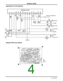
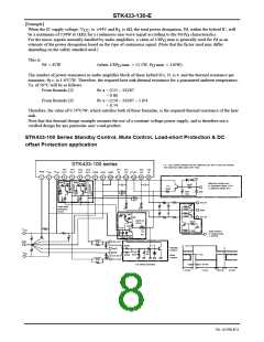
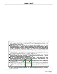
STK433-100 Series Standby Control, Mute Control, Load-short Protection & DC
offset Protection application
STK433-100 series
(*1) The current flowing into the Stand-by pin (#13) must not exceed
the maximum rated value (IST max).
Ch1
Ch1
Ch2
Ch2
Ch1
IN
Ch1
NF
Ch2
NF
Ch2
IN
-PRE -V
1
+V
+PRE SUB GND
ST-BY
13
OUT OUT OUT OUT
CC
CC
2
3
4
6
7
8
9
10
11
12
14
15
5
1kΩ
56kΩ
6.8kΩ
56kΩ
6.8kΩ
Stand-by Control (ex)
H: Operation Mode (+5V)
L: Stand-by Mode (0V)
33kΩ
(*1)
13kΩ
33μF
2kΩ
/10V
Ch2 IN
Load short
protection
circuit
10kΩ
10kΩ
GND
22kΩ
56kΩ
Ch1 IN
Latch up
circuit
10kΩ
1kΩ
0.1μF
+V
CC
2.2kΩ
Mute Control
H: Single Mute
L: Normal
(*4)
R2
10kΩ 100kΩ
Ch2 OUT
GND
-V
82kΩ
+5V
Standby
Control
GND
GND
22μF
22μF
100
kΩ
CC
+5V
82kΩ
Mute
Control
Ch1 OUT
DC offset protection
MUTE
PLAY
ST-BY
MUTE
ST-BY
No. A1596-8/11

 SANYO [ SANYO SEMICON DEVICE ]