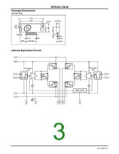
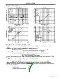
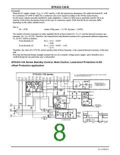
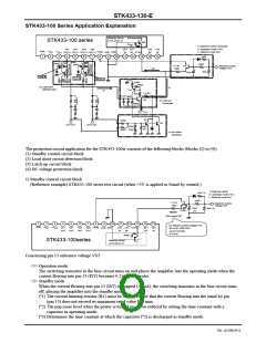
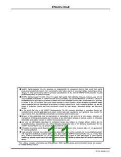
STK433-130-E
2) Load short-circuit detection block
Since the voltage between point B and point C is less than 0.6V in normal operation mode (V
TR2) is not activated, the load short-circuit detection block does not operate.
< 0.6V) and TR1 (or
BE
When a load short-circuit occurs, however, the voltage between point B and point C becomes larger than 0.6V,
causing TR1 (or TR2) to turn on (V
> 0.6V), and current I2 to flows.
BE
3) Latch-up circuit block
TR3 is activated when I2 is supplied to the latch-up circuit.
When TR3 turns on and current I3 starts flowing, VST goes down to 0V (standby mode), protecting the power
amplifier.
Since TR3 and TR4 configure a thyristor, once TR3 is activated, the IC is held in the standby mode.
To release the standby mode and reactivate the power amplifier, it is necessary to set the standby control voltage
temporarily low (0V). Subsequently, when the standby control is returned to high, the power amplifier will become
active again.
(*4) The I3 value varies depending on the supply voltage. Determine the value of R2 using the formula below, so that
I1 is equal to or less than I3.
I1 ≤ I3 = V /R2
CC
4) DC offset protection block
The DC offset protection circuit is activated when 0.5V (typ) voltage is applied to either "OUT CH1" or "OUT
CH2," and the hybrid IC is shut down (standby mode).
To release the IC from the standby mode and reactivate the power amplifier, it is necessary to set the standby control
voltage temporarily low (0V).
Subsequently, when the standby control is returned to high (+5V, for example), the power amplifier will become
active again.
The protection level must be set using the 82kΩ resistor. Furthermore, the time constant must be determined using
22μ//22μ capacitors to prevent the amplifier from malfunctioning due to the audio signal.
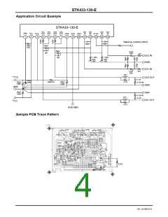
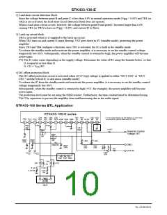
STK433-100 Series BTL Application
STK433-100-E series
Ch1 Ch1 Ch2 Ch2
OUT OUT OUT OUT
Ch1 Ch1
Ch2 Ch2
(*1) The current flowing into the Stand-by pin (#13) must
not exceed the maximum rated value (IST max).
-PRE -V
+V
+PRE SUB GND
ST-BY
IN
NF
NF
IN
CC
CC
1
2
3
4
6
7
8
9
10 11 12 13 14 15
5
100Ω
/1W
0.22Ω
0.22Ω
(*1) R1
100pF
56kΩ
Stand-By Control
Voltage VST
56kΩ
3pF
3pF
100μF
/100V
100μF
/100V
1.8kΩ
1.8kΩ
GND
100Ω/1W
100μF
/100V
10μF
/10V
10μF
/10V
1kΩ
Ch1 IN
2.2μF
/50V
-V
+V
CC
CC
33μF 33μF 56kΩ
3μH
4.7Ω
3μH
4.7Ω
0.1μF
4.7Ω/1W
0.1μF
4.7Ω
/1W
R =8Ω
L
OUT
No. A1596-10/11

 SANYO [ SANYO SEMICON DEVICE ]