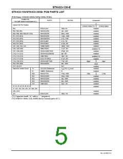
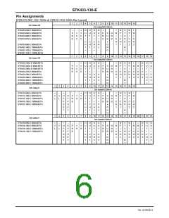
STK433-130-E
Specifications
Absolute maximum ratings at Ta=25°C (excluding rated temperature items), Tc=25°C unless otherwise specified
Parameter
Symbol
Conditions
Ratings
Unit
Maximum quiescent supply voltage 0
Maximum supply voltage 1
Minimum operating supply voltage
Maximum operating flow-in current (pin 13) *7
Thermal resistance
V
V
V
max (0)
When no signal
71.5
62
V
CC
max (1)
min
R ≥6Ω
V
CC
CC
L
10
V
IST OFF max
θj-c
0.6
1.6
150
125
mA
°C/W
°C
Per power transistor
Junction temperature
Tj max
Tc max
Tstg
Both the Tj max and Tc max conditions must be met.
IC substrate operating temperature
Storage temperature
°C
-30 to +125
°C
Allowable load shorted time
*4
ts
V
= 44V, R =6Ω, f=50Hz, P =100W,
CC
L
O
0.3
s
1-channel active
Operating Characteristics at Tc=25°C, R =6Ω, Rg=600Ω, VG=30dB, non-inductive load R , unless otherwise
L
L
specified
Conditions *2
THD
Ratings
typ
Parameter
Symbol
unit
V
f
P
O
CC
min
96
max
(V)
44
44
44
44
44
44
53
53
53
(Hz)
(W)
(%)
0.4
10
Output power
*1
P
P
(1)
(2)
20 to 20k
1k
100
150
O
W
%
O
Total harmonic distortion *1
THD (1)
THD (2)
f , f
20 to 20k
1k
0.4
5.0
VG=30dB
+0 -3dB
0.01
20 to 50k
55
Frequency characteristics *1
Input impedance
1.0
1.0
Hz
kΩ
L
H
ri
1k
Output noise voltage
Quiescent current
*3
V
I
Rg=2.2kΩ
1.0
80
mVrms
mA
NO
No loading
20
45
0
CCO
Output neutral voltage
V
-70
+70
mV
N
Current flowing into pin13 in
IST ON
44
44
Voltage at pin13: 5V,
Current limiting
0
mA
mA
standby mode
*7
Current flowing into pin13 in
IST OFF
resistance R1: 13k
Ω
0.25
0.6
operating mode
*7
[Remarks]
*1: For 1-channel operation
*2: Unless otherwise specified, use a constant-voltage power supply to supply power when inspections are carried out.
*3: The output noise voltage values shown are peak values read with a VTVM. However, an AC stabilized (50Hz)
power supply should be used to minimize the influence of AC primary side flicker noise on the reading.
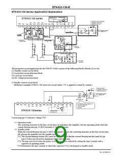
*4: Use the designated transformer power supply circuit shown in the figure below for the measurement of allowable
load shorted time and output noise voltage.
*5: Please connect –Pre V
pin (#1 pin) with the stable minimum voltage and connect so that current does not flow in
CC
by reverse bias.
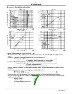
*6: Thermal design must be implemented based on the conditions under which the customer’s end products are expected
to operate on the market.
*7: Be sure to use the current limiting resistor to prevent the current flowing into the standby pin (pin13) never exceeds
the maximum rated value in operating mode.
The circuit is turned on by applying VBE (approximately 0.6V) or higher voltage to the standby pin (pin13).
*8: A thermoplastic adhesive resin is used for this hybrid IC.
DBA40C
10000μF
+V
CC
+
500Ω
Designated transformer power supply
(MG-200 equivalent)
+
500Ω
-V
CC
10000μF
No. A1596-2/11

 SANYO [ SANYO SEMICON DEVICE ]