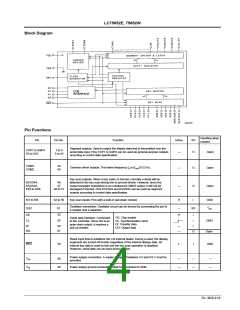
LC75852E, 75852W
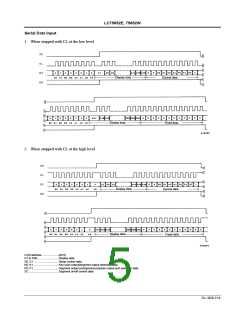
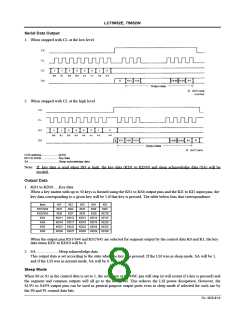
Serial Data Output
1. When stopped with CL at the low level
2. When stopped with CL at the high level
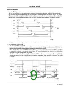
CCB address......................[43H]
KD1 to KD30 ......................Key data
SA ......................................Sleep acknowledge data
Note: If key data is read when DO is high, the key data (KD1 to KD30) and sleep acknowledge data (SA) will be
invalid.
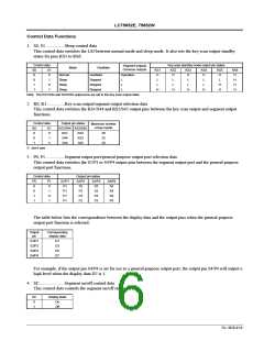
Output Data
1. KD1 to KD30.....Key data
When a key matrix with up to 30 keys is formed using the KS1 to KS6 output pins and the KI1 to KI5 input pins, the
key data corresponding to a given key will be 1 if that key is pressed. The table below lists that correspondence.
Item
KS1/S44
KS2/S45
KS3
KI1
KD1
KD6
KI2
KD2
KD7
KI3
KD3
KD8
KI4
KD4
KD9
KI5
KD5
KD10
KD11 KD12
KD16 KD17
KD21 KD22
KD26 KD27
KD13 KD14 KD15
KD18 KD19 KD20
KD23 KD24 KD25
KD28 KD29 KD30
KS4
KS5
KS6
When the output pins KS1/S44 and KS2/S45 are selected for segment output by the control data K0 and K1, the key
data items KD1 to KD10 will be 0.
2. SA ......................Sleep acknowledge data
This output data is set according to the state when the key was pressed. If the LSI was in sleep mode, SA will be 1,
and if the LSI was in normal mode, SA will be 0.
Sleep Mode
When S0 or S1 in the control data is set to 1, the oscillator at the OSC pin will stop (it will restart if a key is pressed) and
the segment and common outputs will all go to the low level. This reduces the LSI power dissipation. However, the
S1/P1 to S4/P4 output pins can be used as general-purpose output ports even in sleep mode if selected for such use by
the P0 and P1 control data bits.
No. 4828-8/16

 SANYO [ SANYO SEMICON DEVICE ]