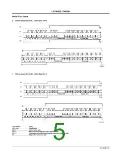
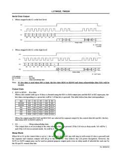
LC75852E, 75852W
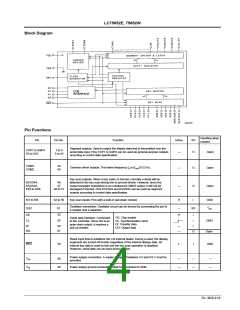
Block Diagram
Pin Functions
Handling when
unused
Pin
Pin No.
Function
Active
—
I/O
O
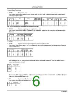
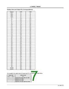
Segment outputs: Used to output the display data that is transmitted over the
serial data input. Pins S1/P1 to S4/P4 can be used as general-purpose outputs
according to control data specification.
S1/P1 to S4/P4
S5 to S43
1 to 4
5 to 43
Open
Open
COM1
COM2
44
45
Common driver outputs. The frame frequency fO is (fOSC/512) Hz.
—
O
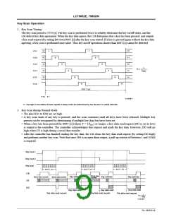
Key scan outputs. When a key matrix is formed, normally a diode will be
attached to the key scan timing line to prevent shorts. However, since the
output transistor impedance is an unbalanced CMOS output, it will not be
damaged if shorted. Pins KS1/S44 and KS2/S45 can be used as segment
outputs according to control data specification.
KS1/S44,
KS2/S45,
KS3 to KS6
46
47
48 to 51
—
H
O
I
Open
KI1 to KI5
52 to 56
57
GND
VDD
Key scan inputs: Pins with a built-in pull-down resistor.
Oscillator connection: Oscillator circuit can be formed by connecting the pin to
a resistor and a capacitor.
OSC
CE
—
H
I/O
I
62
63
CE: Chip enable
CL: Synchronization clock
DI: Transfer data
Serial data interface: Connected
to the controller. Since DO is an
open-drain output, it requires a
pull-up resistor.
GND
CL
DI
I
I
64
61
—
—
DO: Output data
DO
O
Open
Reset input that re-initializes the LSI internal states. During a reset, the display
segments are turned off forcibly regardless of the internal display data. All
internal key data is reset to low and the key scan operation is disabled.
However, serial data can be input during a reset.
RES
59
L
I
GND
Power supply connection. A supply voltage of between 4.5 and 6.0 V must be
provided.
VDD
VSS
60
58
—
—
—
—
—
—
Power supply ground connection. Must be connected to GND.
No. 4828-4/16

 SANYO [ SANYO SEMICON DEVICE ]