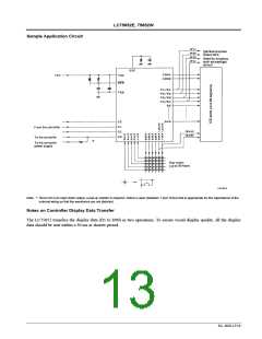
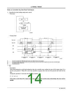
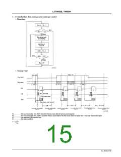
LC75852E, 75852W
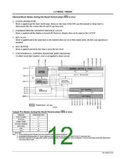
Internal Block States during the Reset Period (when RES is low)
1. CLOCK GENERATOR
Reset is applied and the basic clock stops. However, the state of the OSC pin (the normal or sleep state) is
determined after the control data S0 and S1 has been sent.
2. COMMON DRIVER, SEGMENT DRIVER & LATCH
Reset is applied and the display is turned off. However, display data can be input to the LATCH.
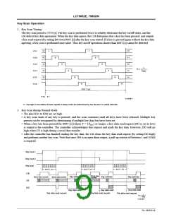
3. KEY SCAN
Reset is applied and at the same time as the internal states are set to their initial states, the key scan operation is
disabled.
4. KEY BUFFER
Reset is applied and all the key data is set to the low level.
5. CCB INTERFACE, CONTROL REGISTER, SHIFT REGISTER
To allow serial data transfers, reset is not applied to these circuits.
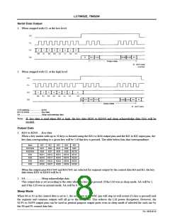
Output Pin States during the Reset Period (when RES is low)
Output pin
S1/P1 to S4/P4
S5 to S43
State during reset
L*3
L
COM1, COM2
KS1/S44, KS2/S45
KS3 to KS5
KS6
L
L*3
X*4
H
DO
H*5
X: don’t care
Note: 3. These output pins are forcibly set to the segment output mode and held low.
4. Immediately following power on, these output pins are undefined until the control data S0 and S1 has been sent.
5. Since this output pin is an open-drain output, a pull-up resistor of between 1 and 10 kΩ is required. This pin is held high during the reset period
even if key data is read.
No. 4828-12/16

 SANYO [ SANYO SEMICON DEVICE ]