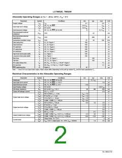
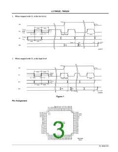
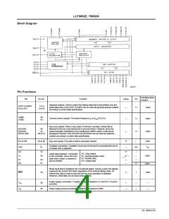
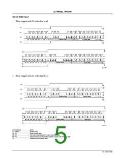
LC75852E, 75852W
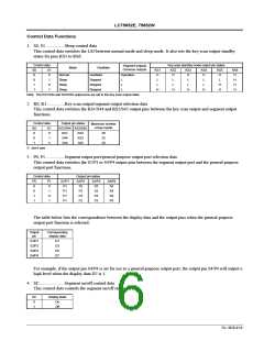
Control Data Functions
1. S0, S1.................Sleep control data
This control data switches the LSI between normal mode and sleep mode. It also sets the key scan output standby
states for pins KS1 to KS6.
Control data
S0 S1
Key scan standby mode output pin states
Segment outputs
Common outputs
Mode
Oscillator
Oscillator
KS1
H
KS2
H
KS3
H
KS4
H
KS5
H
KS6
H
0
0
Normal
Sleep
Sleep
Sleep
Operation
0
1
1
1
0
1
Stopped
Stopped
Stopped
L
L
L
L
L
L
L
L
H
L
L
L
L
H
H
H
H
H
H
H
H
Note: The KS1/S44 and KS2/S45 output pins are set to the key scan output state.
2. K0, K1................Key scan output/segment output selection data
This control data switches the KS1/S44 and KS2/S45 output pins between the key scan output and segment output
functions.
Control data
K0 K1
Output pin states
Maximum number
of key inputs
KS1/S44 KS2/S45
0
0
KS1
S44
S44
KS2
KS2
S45
30
25
20
0
1
1
X
X: don’t care
3. P0, P1.................Segment output port/general-purpose output port selection data
This control data switches the S1/P1 to S4/P4 output pins between the segment output port and the general-purpose
output port functions.
Control data
P0 P1
Output pin states
S1/P1
S1
S2/P2
S2
S3/P3
S3
S4/P4
S4
0
0
0
1
1
1
0
1
P1
P2
S3
S4
P1
P2
P3
S4
P1
P2
P3
P4
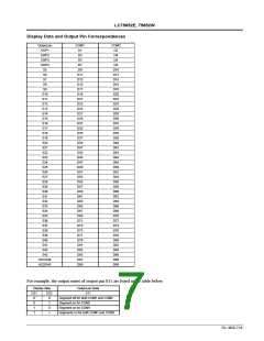
The table below lists the correspondence between the display data and the output pins when the general-purpose
output port function is selected.
Output
pin
Corresponding
display data
S1/P1
S2/P2
S3/P3
S4/P4
D1
D3
D5
D7
For example, if the output pin S4/P4 is set for use as a general-purpose output port, the output pin S4/P4 will output a
high level when the display data D7 is 1.
4. SC.......................Segment on/off control data
This control data controls the segment on/off states.
SC
0
Display state
On
Off
1
No. 4828-6/16

 SANYO [ SANYO SEMICON DEVICE ]