LC72121, 72121M, 72121V
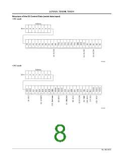
DI Control Data
No.
Control block/data
Function
Related data
• Specifies the divisor for the programmable divider.
This is a binary value in which P15 is the MSB. The LSB changes depending on DVS and SNS.
(* : don’t care)
DVS
SNS
LSB
P0
Set divisor (N)
272 to 65535
272 to 65535
4 to 4095
Actual divisor
Twice the set value
The set value
1
0
0
*
1
0
P0
P4
The set value
Programmable
divider data
* LSB: When P4 is the LSB, P0 to P3 are ignored.
P0 to P15
DVS, SNS
1
• These pins select the signal input to the programmable divider (FMIN or AMIN) and switch the input
frequency range.
(* : don’t care)
DVS
SNS
Input pin Frequency range accepted by the input pin
1
0
0
*
1
0
FMIN
AMIN
AMIN
10 to 160 MHz
2 to 40 MHz
0.5 to 10 MHz
* See the “Structure of the Programmable Divider” section for details.
• Reference frequency selection
R3 R2 R1 R0
Reference frequency
0
0
0
0
0
0
0
0
1
1
1
1
1
1
1
1
0
0
0
0
1
1
1
1
0
0
0
0
1
1
1
1
0
0
1
1
0
0
1
1
0
0
1
1
0
0
1
1
0
1
0
1
0
1
0
1
0
1
0
1
0
1
0
1
100
50
kHz
25
25
12.5
6.25
3.125
3.125
10
Reference divider
data
9
5
2
R0 to R3
XS
1
3
15
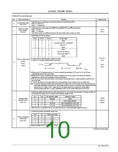
PLL INHIBIT + Xtal OSC STOP
PLL INHIBIT
* PLL INHIBIT mode
In this mode, the programmable divider and the IF counter block are stopped, the FMIN, AMIN, and IFIN
pins are pulled down to ground, and the charge pump output goes to the high-impedance state.
• Crystal oscillator element selection data
XS = 0: 4.5 MHz
XS = 1: 7.2 MHz
Note that 7.2 MHz is selected after a power on reset.
• IF counter measurement start command data
CTE = 1: Starts the counter
CTE = 0: Resets the counter
• Determines the IF counter measurement time.
IF counter control
data
GT1
GT0
Measurement time
Wait time
3 to 4 ms
3 to 4
3
IFS
CTE
0
0
1
1
0
1
0
1
4 ms
8
GT0, GT1
32
7 to 8
64
7 to 8
* See the “Structure of the IF Counter” section for details.
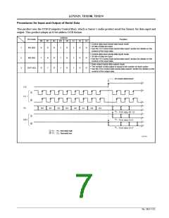
Continued on next page.
No. 5815-9/22

 SANYO [ SANYO SEMICON DEVICE ]