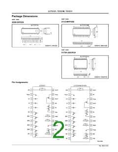
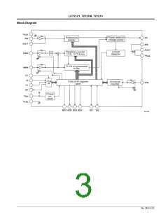
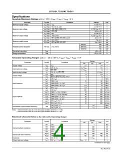
LC72121, 72121M, 72121V
Continued from preceding page.
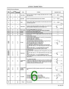
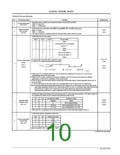
Pin No.
Pin
Type
Function
Equivalent circuit
LC72121M
name
LC72121
LC72121V
• This pin must be set high to enable serial data input (DI) or serial
data output (DO).
CE
DI
3
3
Chip enable
4
5
4
5
Input data
Clock
• Input for serial data transferred from the controller
• Clock used for data synchronization for serial data input (DI) and
serial data output (DO).
CL
• Output for serial data transmitted to the controller. The content of the
data transmitted is determined by DOC0 through DOC2.
DO
6
6
Output data
• LC72121 power supply (VDD 2.7 to 3.6 V)
• The power on reset circuit operates when power is first applied.
VDD
17
18
Power supply
——
VSSX
VSSa
2
2
Ground
Ground
• Ground for the crystal oscillator circuit
——
——
21
22
• Ground for the low-pass filter MOS transistor
• Ground for the LC72121 digital systems other than those that use
VSSd
14
15
Ground
——
VSSa or VSSX
.
• Shared function I/O ports
• The pin function is determined by IOC1 and IOC2 in the serial data.
When the data value 0: Input port
When the data value 1: Output port
• When specified to function as an input port:
The input pin state is reported to the controller through the DO pin.
When the input state is low: The data will be 0:
When the input state is high: The data will be 1:
• When specified to function as an output port:
The output state is determined by IO1 and IO2 in the serial data.
When the data value is 0: The output state will be the open circuit
state.
IO1
IO2
11
13
11
14
I/O port
When the data value is 1: The output state will be a low level.
• These pins are set to input mode after a power on reset.
• Output-only ports
• The output state is determined by BO1 through BO4 in the serial
data.
BO1
BO2
BO3
BO4
7
8
7
8
When the data value is 0: The output state will be the open circuit
state.
When the data value is 1: The output state will be a low level.
• A time base signal (8 Hz) is output from BO1 when TBC in the serial
data is set to 1.
Output port
9
9
10
10
• PLL charge pump output
A high level is output when the frequency of the local oscillator signal
divided by N is higher than the reference frequency, and a low level
is output when that frequency is lower. This pin goes to the high-
impedance state when the frequencies match.
Charge pump
output
PD
18
19
Low-pass filter
amplifier
transistor
AIN
19
20
20
21
• Connections for the MOS transistor used for the PLL active low-pass
filter.
AOUT
• The input frequency range is 0.4 to 12 MHz
• The signal is passed directly to the IF counter.
• The result is output, MSB first, through the DO pin.
• Four measurement periods are supported: 4, 8, 32, and 64 ms.
IFIN
NC
12
—
13
IF counter
12
23
——
NC pin
• No connection
No. 5815-6/22

 SANYO [ SANYO SEMICON DEVICE ]