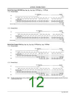
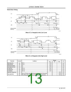
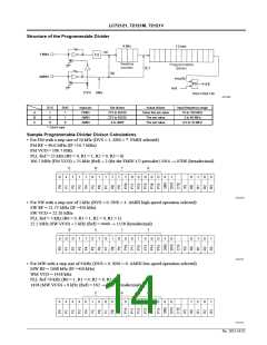
LC72121, 72121M, 72121V
Continued from preceding page.
No.
9
Control block/data
Function
Related data
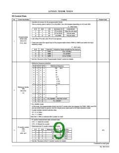
BO1
Clock time base
TBC
• Setting the TBC bit to 1 causes an 8-Hz clock time base signal with a 40% duty to be output from the
BO1 pin. (The BO1 data will be ignored.)
• Forcibly controls the charge pump output.
DLC
Charge pump output
Normal operation
Forced to low
0
1
Charge pump
control data
10
11
DLC
* If the circuit deadlocks due to the VCO control voltage (Vtune) being 0 and the VCO being stopped,
applications can get out of the deadlocked state by setting the charge pump output to low and setting
Vtune to VCC. (Deadlock clear circuit)
IF counter control
data
• This data is normally set to 1. Setting this data to 0 sets the circuit to reduced input sensitivity mode, in
which the sensitivity is reduced by about 10 to 30 mV rms.
* See the “IF Counter Operation” section for details.
IFS
• Test data
TEST0
Test data
12
13
TEST1
TEST2
All these bits must be set to 0.
TEST0 to 2
All these bits are set to 0 after a power on reset.
DNC
• This bit must be set to 0.
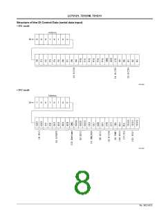
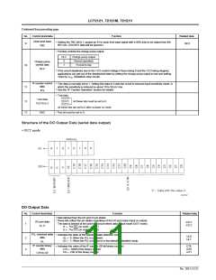
Structure of the DO Output Data (serial data output)
• OUT mode
DO Output Data
No. Control block/data
Function
Related data
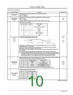
• Data latched from the I/O port IO pin states.
• These bits reflect the pin states regardless of the I/O port mode (input or output).
The data is latched at the point the circuit enters data output mode (OUT mode).
I/O port data
12, I1
IOC1
IOC2
1
I1 ← The IO1 pin state
I2 ← The IO2 pin state
H : 1
L : 0
PLL unlocked state
data
• Indicates the state of the unlocked state detection circuit.
UL ← 0: When the PLL is unlocked.
UL0
UL1
2
3
UL ← 1: When the PLL is locked or in the detection disabled mode.
UL
IF counter binary
data
• Indicates the value of the IF counter (20-bit binary counter).
C19 ← MSB of the binary counter
CTE
GT0
GT1
C0 ← LSB of the binary counter
C19 to C0
No. 5815-11/22

 SANYO [ SANYO SEMICON DEVICE ]