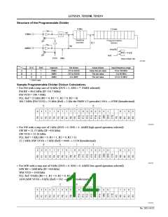
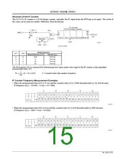
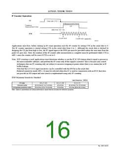
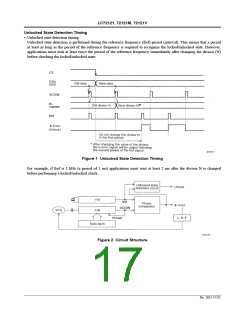
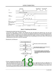
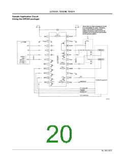
LC72121, 72121M, 72121V
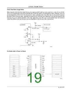
Clock Time Base Usage Notes
When using the clock time base output function, the output pin (BO1) pull-up resistor must have a value of over 100 kΩ.
The use of a Schmitt input in the microcontroller that accepts this signal is recommended to reduce chattering. This is to
prevent degradation of the VCO C/N characteristics when combining with a loop filter that uses the internal transistor
provided to form a low-pass filter. Although the ground for the clock time base output pin (V ) and the ground for the
SSd
transistor (V ) are isolated internally on the chip, applications must take care to avoid ground loops and minimize
SSa
current fluctuations in the time base pin to prevent degradation of the low-pass filter characteristics.
Pin States after a Power on Reset
No. 5815-19/22

 SANYO [ SANYO SEMICON DEVICE ]