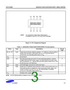
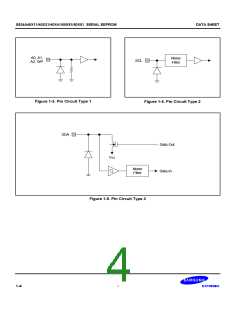
DATA SHEET
S524A40X11/40X21/40X41/60X81/60X51 SERIAL EEPROM
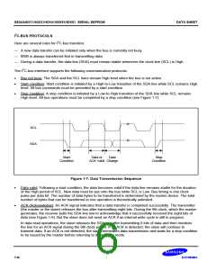
Master
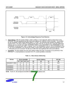
SCL Line
Bit 1
Bit 9
Data from
Transmitter
ACK from
Receiver
ACK
Figure 1-8. Acknowledge Response From Receiver
·
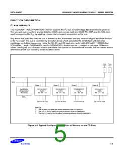
Slave Address: After the master initiates a Start condition, it must output the address of the device to be
accessed. The most significant four bits of the slave address are called the “device identifier”. The identifier
for the S524A40X11/40X21/40X41/60X81/60X51 is “1010B”. The next three bits comprise the address of a
specific device. The device address is defined by the state of the A0, A1 and A2 pins. Using this addressing
scheme, you can cascade up to eight S524A40X11/40X21 or four S524A40X41 or two S524A60X81 or one
S524A60X51 on the bus (see Table 1-2 below). The b1 for S524A40X41 or the b1, b2 for S524A60X81 or the
b1, b2, b3 for S524A60X51 are used by the master to select which of the blocks of internal memory (1 block
= 256 words) are to be accessed. The bits are in effect the most significant bits of the word address.
·
Read/Write: The final (eighth) bit of the slave address defines the type of operation to be performed. If the
R/W bit is “1”, a read operation is executed. If it is “0”, a write operation is executed.
Table 1-2. Slave Device Addressing
Device
Device Identifier
Device Address
R/W Bit
b0
b7 b6 b5 b4
b3
b2
b1
S524A40X11/40X2
1
1
0
1
0
A2
A1
A0
R/W
S524A40X41
S524A60X81
S524A60X51
1
1
1
0
0
0
1
1
1
0
0
0
A2
A2
B2
A1
B1
B1
B0
B0
B0
R/W
R/W
R/W
NOTE: The B2, B1, B0 correspond to the MSB of the memory array address word.
1-7

 SAMSUNG [ SAMSUNG ]