DATA SHEET
S524A40X11/40X21/40X41/60X81/60X51 SERIAL EEPROM
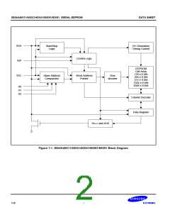
FUNCTION DESCRIPTION
I2C-BUS INTERFACE
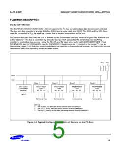
The S524A40X11/40X21/40X41/60X81/60X51 supports the I2C-bus serial interface data transmission protocol.
The two-wire bus consists of a serial data line (SDA) and a serial clock line (SCL). The SDA and the SCL lines
must be connected to VCC by a pull-up resistor that is located somewhere on the bus.
Any device that puts data onto the bus is defined as the “transmitter” and any device that gets data from the bus
is the “receiver.” The bus is controlled by a master device which generates the serial clock and start/stop
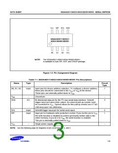
conditions, controlling bus access. Using the A0, A1, and A2 input pins, up to eight S524A40X11/40X21 (four
S524A40X41, two for S524A60X81, one for S524A60X51) devices can be connected to the same I2C-bus as
slaves (see Figure 1-6). Both the master and slaves can operate as transmitter or receiver, but the master device
determines which bus operating mode would be active.
VCC
VCC
R
R
SDA
SCL
Slave 1
S524A40X21
Slave 2
S524A40X21
Slave 3
S524A40X21
Slave 8
S524A40X21
Bus Master
(Transmitter/
Receiver)
Tx/Rx
A0 A1 A2
Tx/Rx
A0 A1 A2
Tx/Rx
A0 A1 A2
Tx/Rx
A0 A1 A2
MCU
To VCC or VSS
To VCC or VSS
To VCC or VSS
To VCC or VSS
NOTES:
1. The A0 does not affect the device address of the S524A40X41.
2. The A0, A1 do not affect the device address of the S524A60X81.
3. The A0, A1, and A2 do not affect the device address of the S524A60X51.
Figure 1-6. Typical Configuration (16 Kbits of Memory on the I2C-Bus)
1-5

 SAMSUNG [ SAMSUNG ]