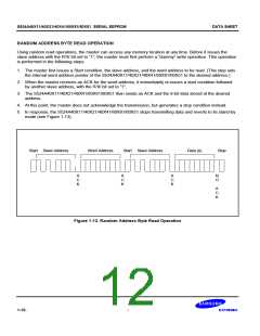
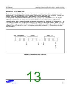
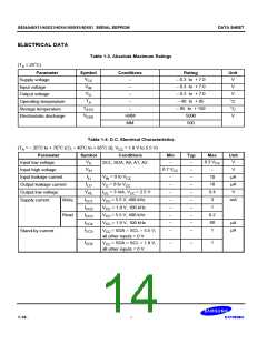
DATA SHEET
S524A40X11/40X21/40X41/60X81/60X51 SERIAL EEPROM
HARDWARE-BASED WRITE PROTECTION
You can also write-protect the entire memory area of the S524A40X11/40X21/40X41/60X81/60X51. This method
of write protection is controlled by the state of the Write Protect (WP) pin.
When the WP pin is connected to VCC, any attempt to write a value to the memory is ignored.
The S524A40X11/40X21/40X41/60X81/60X51 will acknowledge slave and word address, but it will not generate
an acknowledge after receiving the first byte of the data. Thus the write cycle will not be started when the stop
condition is generated. By connecting the WP pin to VSS, the write function is allowed for the entire memory.
These write protection features effectively change the EEPROM to a ROM in order to prevent data from being
overwritten. Whenever the write function is disabled, a slave address and a word address are acknowledged on
the bus, but data bytes are not acknowledged.
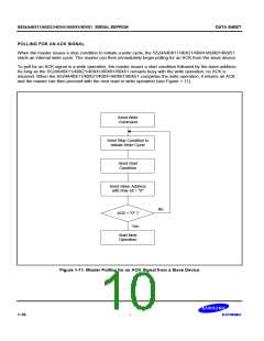
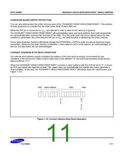
CURRENT ADDRESS BYTE READ OPERATION
The internal word address pointer maintains the address of the last word accessed, incremented by one.
Therefore, if the last access (either read or write) was to the address “n”, the next read operation would access
data at address “n+1”.
When the S524A40X11/40X21/40X41/60X81/60X51 receives a slave address with the R/W bit set to “1”, it issues
an ACK and sends the eight bits of data. The master does not acknowledge the transfer but it does generate a
Stop condition. In this way, the S524A40X11/40X21/40X41/60X81/60X51 effectively stops the transmission (see
Figure 1-12).
Start Slave Address
Data
Stop
A
C
K
N
O
A
C
K
Figure 1-12. Current Address Byte Read Operation
1-11

 SAMSUNG [ SAMSUNG ]