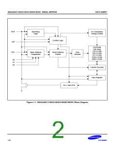
DATA SHEET
S524A40X11/40X21/40X41/60X81/60X51 SERIAL EEPROM
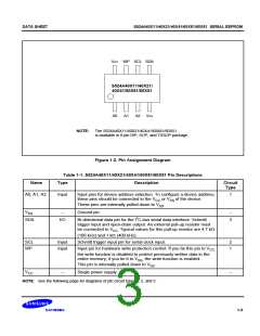
VCC WP SCL SDA
S524A40X11/40X21/
40X41/60X81/60X51
A0
A1
A2
VSS
NOTE:
The S524A40X11/40X21/40X41/60X81/60X51
is available in 8-pin DIP, SOP, and TSSOP package.
Figure 1-2. Pin Assignment Diagram
Table 1-1. S524A40X11/40X21/40X41/60X81/60X51 Pin Descriptions
Name
Type
Description
Circuit
Type
A0, A1, A2
Input
Input pins for device address selection. To configure a device address,
these pins should be connected to the VCC or VSS of the device.
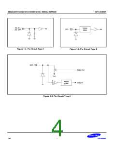
1
These pins are internally pulled down to VSS
.
VSS
–
Ground pin.
–
3
SDA
I/O
Bi-directional data pin for the I2C-bus serial data interface. Schmitt
trigger input and open-drain output. An external pull-up resistor must
be connected to VCC. Typical values for this pull-up resistor are 4.7 kW
(100 kHz) and 1 kW (400 kHz).
SCL
WP
Input
Input
Schmitt trigger input pin for serial clock input.
Input pin for hardware write protection control. If you tie this pin to VCC,
2
1
the write function is disabled to protect previously written data in the
entire memory; if you tie it to VSS, the write function is enabled.
This pin is internally pulled down to VSS
.
VCC
–
Single power supply.
–
NOTE: See the following page for diagrams of pin circuit types 1, 2, and 3.
1-3

 SAMSUNG [ SAMSUNG ]