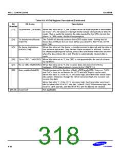
HDLC CONTROLLERS
S3C4510B
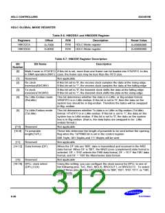
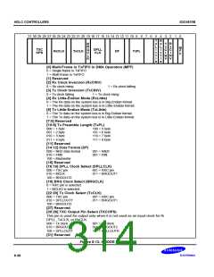
31 30 29 28 27 26 25 24 23 22 21 20 19 18 17 16 15 14 13 12 11 10 9
8
7
6
5
4
3
2
1
0
T
x
L
i
R
x
L
i
R
x
C
I
B
R
G
C
L
T
x
C
I
M
F
F
TXC
OPS
DPLL
CLK
RxCLK
TxCLK
DF
TxPL
t
t
t
t
N
N
l
K
l
V V
e
e
[0] Muilt-Frame in TxFIFO in DMA Operation (MFF)
0 = Single frame in TxFIFO
1 = Multi frame in TxFIFO
[1] Reserved
[2] Rx Clock Inversion (RxCINV)
0 = Rx clock rising
1 = Rx clock falling
[3] Tx Clock Inversion (TxCINV)
0 = Tx clock falling
1 = Tx clock rising
[4] Rx Little-Endian Mode (RxLittle)
0 = The Rx data on the system bus is in Big-Endian format.
1 = The Rx data on the system bus is in Little-Endian format.
[5] Tx Little-Endian Mode (TxLittle)
0 = The Tx data on the system bus is in Big-Endian format.
1 = The Tx data on the system bus is in Little-Endian format.
[7:6] Reserved
[10:8] Tx Preamble Length (TxPL)
000 = 1 byte
001 = 2 byte
010 = 3 byte
011 = 4 byte
100 = 5 byte
101 = 6 byte
110 = 7 byte
111 = 8 byte
[11] Reserved
[14:12] Data Format (DF)
000 = NRZ data format
010 = FM0
001 = NRZI
001 = FMI
100 = Machester
[15] Reserved
[18:16] DPLL Clock Select (DPLLCLK)
000 = TXC pin
001 = RXC pin
010 = MCLK
011 = BRGOUT1
100 = BRGOUT2
[19] BRG Clock Select (BRGCLK)
0 = RXC pin is selected.
1 = MCLK2 is selected.
[22:20] Tx Clock Select (TxCLK)
000 = TXC pin
001 = RXC pin
010 = DPLLOUTT
100 = BRGOUT2
[27] Reserved
011 = BRGOUT1
[30:28] TXC Output Pin Select (TXCOPS)
This pin is used for output only when it is not used as an input clock for th
DPLL, TxCLK, or RxCLK.
000 = Tx clock
001 = Rx clock
010 = BRGOUT1
100 = DPLLOUTT
[31] Reserved
011 = BRGOUT2
101 = DPLLOUTR
Figure 8-13. HMODE Register
8-28

 SAMSUNG [ SAMSUNG ]