SYSTEM MANAGER
S3C4510B
SYSTEM MANAGER REGISTERS
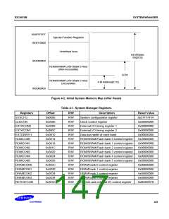
To control external memory operations, the System Manager uses a dedicated set of special registers (see Table
4-1). By programming the values in the System Manager special registers, you can specify such things as
·
·
·
·
·
Memory type
External bus width access cycle
Control signal timing (RAS and CAS, for example)
Memory bank locations
The sizes of memory banks to be used for arbitrary address spacing
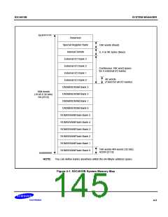
The System Manager uses special register settings to control the generation and processing of the control
signals, addresses, and data that are required by external devices in a standard system configuration. Special
registers are also used to control access to ROM/SRAM/Flash banks, up to four DRAM banks and four external
I/O banks, and a special register mapping area.
The address resolution for each memory bank base pointer is 64K-bytes (16 bits). The base address pointer is 10
bits. This gives a total addressable memory bank space of 16 M words.
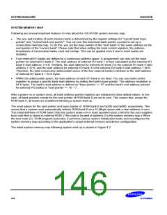
NOTE
When writing a value to a memory bank control register from ROMCON0 to REFEXTCON (locations
0x3014 to 0x303C), as shown in Table 4-1, you must always set the register using a single STM (Store
Multiple) instruction. Additionally, the address spaces for successive memory banks must not overlap in
the system memory map.
4-2

 SAMSUNG [ SAMSUNG ]