DDR2 SDRAM
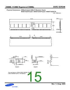
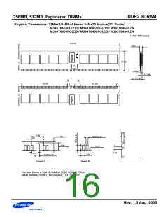
256MB, 512MB Registered DIMMs
Electrical Characteristics & AC Timing for DDR2-667/533/400 SDRAM
(0 °C < T
< 95 °C; V
= 1.8V + 0.1V; V = 1.8V + 0.1V)
DDQ DD
CASE
Refresh Parameters by Device Density
Parameter
Symbol
256Mb
512Mb
1Gb
2Gb
4Gb
Units
Refresh to active/Refresh command time
tRFC
tREFI
75
105
127.5
195
tbd
ns
0 °C ≤ T
≤ 85°C
≤ 95°C
7.8
3.9
7.8
3.9
7.8
3.9
7.8
3.9
7.8
3.9
µs
µs
CASE
Average periodic refresh interval
85 °C < T
CASE
Speed Bins and CL, tRCD, tRP, tRC and tRAS for Corresponding Bin
Speed
Bin (CL - tRCD - tRP)
Parameter
tCK, CL=3
tCK, CL=4
tCK, CL=5
tRCD
DDR2-667(E6)
DDR2-533(D5)
DDR2-400(CC)
3 - 3 - 3
5 - 5 - 5
4 - 4 - 4
Units
min
max
min
max
min
max
5
3.75
3
8
8
8
5
3.75
-
8
8
-
5
5
8
8
-
ns
ns
ns
ns
ns
ns
ns
-
15
15
54
39
15
15
55
40
15
15
55
40
tRP
tRC
tRAS
70000
70000
70000
Timing Parameters by Speed Grade
(Refer to notes for informations related to this table at the bottom)
DDR2-667
DDR2-533
DDR2-400
Symbol
Units Notes
Parameter
min
-450
max
min
max
+500
+450
0.55
0.55
x
min
-600
-500
0.45
0.45
max
+600
+500
0.55
0.55
x
DQ output access time from CK/CK
DQS output access time from CK/CK
CK high-level width
tAC
+450
+400
0.55
0.55
x
-500
ps
ps
tDQSCK
tCH
-400
-450
0.45
0.45
tCK
tCK
ps
CK low-level width
tCL
0.45
0.45
CK half period
tHP
min(tCL, tCH)
3000
min(tCL, tCH)
3750
min(tCL, tCH)
5000
Clock cycle time, CL=x
tCK
8000
x
8000
x
8000
x
ps
DQ and DM input hold time
DQ and DM input setup time
tDH
175
225
275
ps
tDS
50
x
100
x
150
x
ps
Control & Address input pulse width for each
input
tIPW
0.6
x
0.6
x
0.6
x
tCK
DQ and DM input pulse width for each input
Data-out high-impedance time from CK/CK
DQS low-impedance time from CK/CK
DQ low-impedance time from CK/CK
tDIPW
tHZ
0.35
x
x
0.35
x
x
0.35
x
x
tCK
ps
tAC max
tAC max
tAC max
tAC max
tAC max
tAC max
tAC max
tAC max
tAC max
tLZ(DQS)
tLZ(DQ)
tAC min
2*tAC min
tAC min
2* tACmin
tAC min
2* tACmin
ps
ps
DQS-DQ skew for DQS and associated DQ
signals
tDQSQ
x
250
x
300
x
350
ps
DQ hold skew factor
tQHS
tQH
x
350
x
400
x
450
ps
ps
DQ/DQS output hold time from DQS
tHP - tQHS
WL-0.25
0.35
x
WL+0.25
x
tHP - tQHS
WL-0.25
0.35
x
WL+0.25
x
tHP - tQHS
WL-0.25
0.35
x
WL+0.25
x
Write command to first DQS latching transition tDQSS
DQS input high pulse width tDQSH
tCK
tCK
Rev. 1.3 Aug. 2005

 SAMSUNG [ SAMSUNG ]