DDR2 SDRAM
256MB, 512MB Registered DIMMs
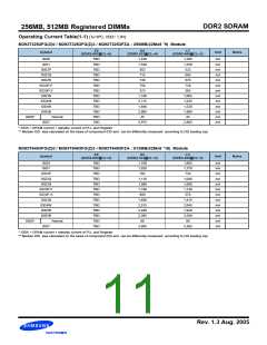
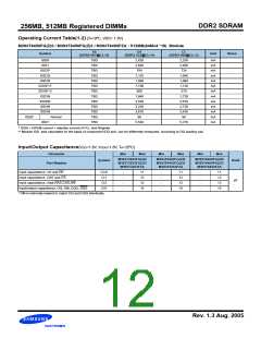
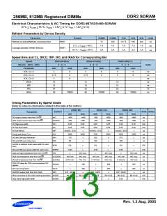
Operating Current Table(1-2) (TA=0oC, VDD= 1.9V)
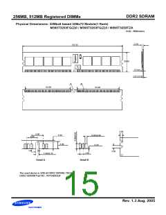
M393T6450FG(Z)0 / M393T6450FG(Z)3 / M393T6450FZA : 512MB(64Mx4 *18) Module
E6
D5
CC
Symbol
Unit
Notes
(DDR2-667@CL=5)
(DDR2-533@CL=4)
(DDR2-400@CL=3)
IDD0
IDD1
TBD
TBD
TBD
TBD
TBD
TBD
TBD
TBD
TBD
TBD
TBD
TBD
TBD
2,420
2,640
784
1,110
1,090
1,190
600
1,840
3,550
3,230
3,610
90
2,250
2,400
724
1,040
1,060
1,130
570
1,730
2,810
2,730
3,430
90
mA
mA
mA
mA
mA
mA
mA
mA
mA
mA
mA
mA
mA
IDD2P
IDD2Q
IDD2N
IDD3P-F
IDD3P-S
IDD3N
IDD4W
IDD4R
IDD5B
IDD6*
Normal
IDD7
5,540
5,210
* IDD6 = DRAM current + standby current of PLL and Register
** Module IDD was calculated on the basis of component IDD and can be differently measured according to DQ loading cap.
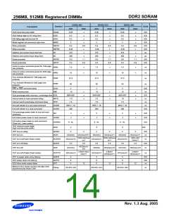
Input/Output Capacitance(VDD=1.8V, VDDQ=1.8V, TA=25oC)
Parameter
Min
Max
Min
Max
Min
Max
M393T3253FG(Z)0
M393T3253FG(Z)3
M393T3253FZA
M393T6453FG(Z)0
M393T6453FG(Z)3
M393T6453FZA
M393T6450FG(Z)0
M393T6450FG(Z)3
M393T6450FZA
Symbol
Units
Part-Number
Input capacitance, CK and CK
CCK
CI1
-
-
-
-
11
12
12
10
-
-
-
-
11
12
12
10
-
-
-
-
11
12
12
10
Input capacitance, CKE and CS
pF
Input capacitance, Addr,RAS,CAS,WE
Input/output capacitance, DQ, DM, DQS, DQS
CI2
CIO
* DM is internally loaded to match DQ and DQS identically.
Rev. 1.3 Aug. 2005

 SAMSUNG [ SAMSUNG ]