DDR2 SDRAM
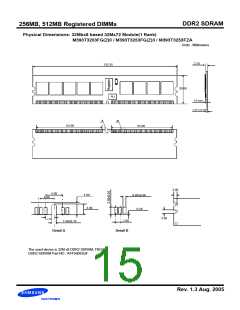
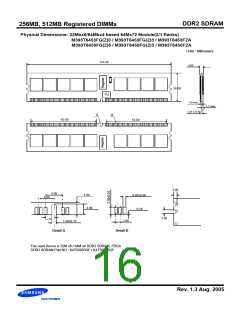
256MB, 512MB Registered DIMMs
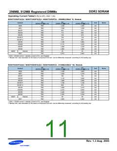
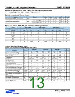
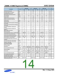
DDR2-667
DDR2-533
DDR2-400
Symbol
Units Notes
Parameter
min
0.35
0.2
0.2
2
max
x
min
max
x
min
0.35
0.2
0.2
2
max
x
DQS input low pulse width
tDQSL
tDSS
tDSH
tMRD
tWPST
tWPRE
tIH
0.35
0.2
0.2
2
tCK
tCK
tCK
tCK
tCK
tCK
ps
DQS falling edge to CK setup time
DQS falling edge hold time from CK
Mode register set command cycle time
Write postamble
x
x
x
x
x
x
x
x
x
0.4
0.35
275
200
0.9
0.4
0.6
x
0.4
0.35
375
250
0.9
0.4
0.6
x
0.4
0.35
475
350
0.9
0.4
0.6
x
Write preamble
Address and control input hold time
Address and control input setup time
Read preamble
x
x
x
tIS
x
x
x
ps
tRPRE
tRPST
1.1
0.6
1.1
0.6
1.1
0.6
tCK
tCK
Read postamble
Active to active command period for 1KB page
size products
tRRD
7.5
10
x
x
7.5
10
x
x
7.5
10
x
x
ns
ns
ns
ns
Active to active command period for 2KB page
size products
tRRD
tFAW
Four Activate Window for 1KB page size
products
37.5
50
37.5
50
37.5
50
Four Activate Window for 2KB page size
products
tFAW
CAS to CAS command delay
Write recovery time
tCCD
tWR
2
15
2
15
2
15
tCK
ns
x
x
x
x
x
x
x
x
x
Auto precharge write recovery + precharge time tDAL
tWR+tRP
7.5
tWR+tRP
7.5
tWR+tRP
10
tCK
ns
Internal write to read command delay
Internal read to precharge command delay
Exit self refresh to a non-read command
Exit self refresh to a read command
tWTR
tRTP
7.5
7.5
7.5
ns
tXSNR
tXSRD
tRFC + 10
200
tRFC + 10
200
tRFC + 10
200
ns
tCK
Exit precharge power down to any non-read
command
tXP
2
2
x
x
2
2
x
x
2
2
x
x
tCK
tCK
tCK
Exit active power down to read command
tXARD
tXARDS
Exit active power down to read command
(Slow exit, Lower power)
6 - AL
6 - AL
6 - AL
CKE minimum pulse width
(high and low pulse width)
tCKE
tCK
3
3
3
ODT turn-on delay
ODT turn-on
tAOND
tAON
2
2
2
2
2
2
tCK
ns
tAC(min)
tAC(max)+0.7
tAC(min)
tAC(max)+1
tAC(min)
tAC(max)+1
2tCK+tAC(ma
x)+1
2tCK+tAC(ma
x)+1
2tCK+tAC
(max)+1
ODT turn-on(Power-Down mode)
ODT turn-off delay
tAONPD
tAOFD
tAOF
tAC(min)+2
2.5
tAC(min)+2
2.5
tAC(min)+2
2.5
ns
tCK
ns
2.5
2.5
2.5
tAC(max)+
0.6
ODT turn-off
tAC(min)
tAC(min)
tAC(max)+ 0.6
tAC(min)
tAC(max)+ 0.6
2.5tCK+tAC(
max)+1
2.5tCK+
2.5tCK+
ODT turn-off (Power-Down mode)
tAOFPD
tAC(min)+2
tAC(min)+2
tAC(min)+2
ns
tAC(max)+1
tAC(max)+1
ODT to power down entry latency
ODT power down exit latency
OCD drive mode output delay
tANPD
tAXPD
tOIT
3
8
0
3
8
0
3
8
0
tCK
tCK
ns
12
12
12
Minimum time clocks remains ON after CKE
asynchronously drops LOW
tDelay
tIS+tCK +tIH
tIS+tCK +tIH
tIS+tCK +tIH
ns
Rev. 1.3 Aug. 2005

 SAMSUNG [ SAMSUNG ]