DDR2 SDRAM
256MB, 512MB Registered DIMMs
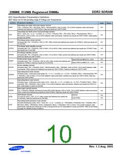
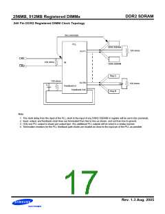
240 Pin DDR2 Registered DIMM Clock Topology
0ns (nominal)
PLL
DDR2 SDRAM
120 ohms
OUT1
CK0
120 ohms
IN
DDR2 SDRAM
Reg.A
CK0
120 ohms
OUTN
120 ohms
C
C
Feedback In
Feedback Out
Reg.B
Note:
1. The clock delay from the input of the PLL clock to the input of any DDR2 SDRAM or register will be set to 0ns (nominal).
2. Input, output, and feedback clock lines are terminated from line to line as shown, and not from line to ground.
3. Only one PLL output is shown per output type. Any additional PLL outputs will be wired in a similar manner.
4. Termination resistors for the PLL feedback path clocks are located as close to the input pin of the PLL as possible.
Rev. 1.3 Aug. 2005

 SAMSUNG [ SAMSUNG ]