512MB, 1GB, 2GB Registered DIMMs
DDR2 SDRAM
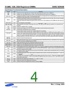
Input/Output Functional Description
Symbol
CK0
Type
Input
Input
Function
Positive line of the differential pair of system clock inputs that drives input to the on-DIMM PLL.
Negative line of the differential pair of system clock inputs that drives the input to the on-DIMM PLL.
CK0
Activates the SDRAM CK signal when high and deactivates the CK signal when low. By deactivating the clocks, CKE low
initiates the Power Down mode, or the Self Refresh mode.
CKE0~CKE1
S0~S1
Input
Enables the associated SDRAM command decoder when low and disables decoder when high. When decoder is disabled,
new commands are ignored but previous operations continue.
These input signals also disable all outputs (except CKE and ODT) of the register(s) on the DIMM when both inputs are
high.
Input
ODT0~ODT1
Input
Input
I/O bus impedance control signals.
When sampled at the positive rising edge of the clock, CAS, RAS, and WE define the operation to be executed by the
SDRAM.
RAS, CAS, WE
V
Supply
Supply
Input
Reference voltage for SSTL_18 inputs
REF
V
Isolated power supply for the DDR SDRAM output buffers to provide improved noise immunity
Selects which SDRAM bank of four is activated.
DDQ
BA0~BA1
During a Bank Activate command cycle, Address defines the row address.
During a Read or Write command cycle, Address defines the column address. In addition to the column address, AP is
used to invoke autoprecharge operation at the end of the burst read or write cycle. If AP is high, autoprecharge is selected
and BA0, BA1 defines the bank to be precharged. If AP is low, autoprecharge is disabled. During a Precharge command
cycle, AP is used in conjunction with BA0, BA1 to control which bank(s) to precharge. If AP is high, all banks will be pre-
charged regardless of the state of BA0 or BA1. If AP is low, BA0 and BA1 are used to define which bank to precharge.
A0~A9,A10/AP
A11~A13
Input
DQ0~63,
In/Out
Input
Data and Check Bit Input/Output pins
CB0~CB7
Masks write data when high, issued concurrently with input data. Both DM and DQ have a write latency of one clock once
the write command is registered into the SDRAM.
DM0~DM8
V
, V
Supply
In/Out
In/Out
Input
Power and ground for the DDR SDRAM input buffers and core logic
Positive line of the differential data strobe for input and output data.
Negative line of the differential data strobe for input and output data.
DD
SS
DQS0~DQS17
DQS0~DQS17
SA0~SA2
These signals are tied at the system planar to either V or V
to configure the serial SPD EEPROM address range.
DDSPD
SS
This bidirectional pin is used to transfer data into or out of the SPD EEPROM. A resistor must be connected from the SDA
bus line to V to act as a pullup.
SDA
SCL
In/Out
Input
DDSPD
This signal is used to clock data into and out of the SPD EEPROM. A resistor may be connected from the SCL bus time
to V to act as a pullup.
DDSPD
Serial EEPROM positive power supply (wired to a separate power pin at the connector which supports from 1.7 Volt to 3.6
Volt operation).
V
Supply
DDSPD
The RESET pin is connected to the RST pin on the register and to the OE pin on the PLL. When low, all register outputs
will be driven low and the PLL clocks to the DRAMs and register(s) will be set to low level (The PLL will remain synchro-
nized with the input clock )
RESET
Input
Par_In
Err_Out
TEST
Input
Input
Parity bit for the Address and Control bus. ( “1 “ : Odd, “0 “ : Even)
Parity error found in the Address and Control bus
In/Out
Used by memory bus analysis tools (unused on memory DIMMs)
Rev. 1.2 Aug. 2005

 SAMSUNG [ SAMSUNG ]