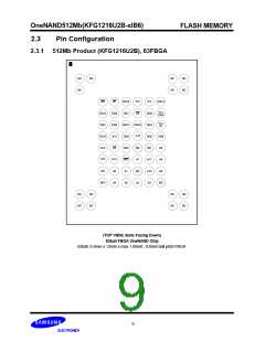
OneNAND512Mb(KFG1216U2B-xIB6)
1.4 Product Features
FLASH MEMORY
Device Architecture
B die
3.3V(2.7V to 3.6V)
16 bit
1KB BootRAM, 4KB DataRAM
(2K+64)B Page Size, (128K+4K)B Block Size
•
•
•
•
•
Design Technology:
Supply Voltage:
Host Interface:
5KB Internal BufferRAM:
SLC NAND Array:
Device Performance
Synchronous Burst Read
•
Host Interface Type:
- Up to 66MHz clock frequency
- Linear Burst 4-, 8-, 16-, 32-words with wrap around
- Continuous 1K words Sequential Burst
Asynchronous Random Read
- 76ns access time
Asynchronous Random Write
Latency 3,4(Default),5,6 and 7.
1~40MHz : Latency 3 available
1~66MHz : Latency 4,5,6 and 7 available
Up to 4 sectors using Sector Count Register
Cold/Warm/Hot/NAND Flash Core Reset
up to 64 Blocks
•
Programmable Burst Read Latency:
•
•
•
•
Multiple Sector Read/Write:
Multiple Reset Modes:
Multi Block Erase:
Typical Power,
Low Power Dissipation:
- Standby current : 35uA@3.3V
- Synchronous Burst Read current(66MHz) : 25mA @ 3.3V
- Load current : 30mA @ 3.3V
- Program current : 28mA @ 3.3V
- Erase current : 23mA @ 3.3V
- Multi Block Erase current : 23mA @ 3.3V
- Endurance : 100K Program/Erase Cycles
- Data Retention : 10 Years
• Reliable CMOS Floating-Gate Technology
System Hardware
• Voltage detector generating internal reset signal from Vcc
•
•
Hardware reset input (RP)
Data Protection Modes
- Write Protection for BootRAM
- Write Protection for NAND Flash Array
- Write Protection during power-up
- Write Protection during power-down
- 1st block OTP
•
•
•
•
User-controlled One Time Programmable(OTP) area
Internal 2bit EDC / 1bit ECC
Internal Bootloader supports Booting Solution in system
Handshaking Feature
- INT pin indicates Ready / Busy
- Polling the interrupt register status bit
- by ID register
•
Detailed chip information
Packaging
512Mb products
63ball, 9.5mm x 12mm x max 1.0mmt , 0.8mm ball pitch FBGA
67ball, 7.0mm x 9mm x max 1.0mmt , 0.8mm ball pitch FBGA
•
5

 SAMSUNG [ SAMSUNG ]