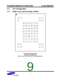
OneNAND512Mb(KFG1216U2B-xIB6)
FLASH MEMORY
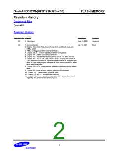
Revision History
Document Title
OneNAND
Revision History
Revision No. History
Draft Date
Remark
0.0
1. Initial issue.
Aug. 29, 2006
Advanced
1.0
1. Corrected errata
Jan. 15, 2007
Final
2. Deleted Sync Burst Write, Cache Read, Sync Burst Block Read and
83Mhz option.
3. Added package size of 7mm x 9mm (67ball)
4. Chapter 2.8.19 : revised description of RDY configuration.
5. Chapter 3.1 : added comments on Note 4)
6. Chapter 3.3 : revised Start Block Address value at Hot reset into N/A.
7. Chapter 3.4.4 & 3.83.8 & 3.9 & 3.10.1 & 3.10.3 : revised flow charts of
’Data protection operation’ & ’All block unlock operation’ & ’Program oper-
ation’ & ’Copy-back program operation’ & ’Block erase operation’ & ’Multi-
block erase verify read’.
8. Chapter 3.5 & 6.17 : corrected data protection explanation during power-
down.
9. Chapter 3.9 : corrected start address restriction of DataRAMs.
10. Chapter 3.9.1 : deleted data sequence table.
11. Chapter 6.11 & 6.12 : revised timing diagram.
12. Chapter 7.1 & 7.1.2 : added the case table of INT type and comment
regarding INT pin connection when unused.
2

 SAMSUNG [ SAMSUNG ]