OneNAND512Mb(KFG1216U2B-xIB6)
FLASH MEMORY
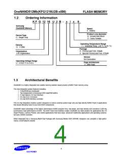
1.2
Ordering Information
K F G 12 16 U 2 B - x I x 6
Samsung
OneNAND Memory
Speed
6 : 66MHz
Product Line desinator
B : Include Bad Block
D : Daisy Sample
Device Type
G : Single Chip
Operating Temperature Range
I = Industrial Temp. (-40 °C to 85 °C)
Density
12 : 512Mb
Package
D : FBGA(Lead Free, 63ball)
S : Special FBGA(Lead Free, 67ball)
Organization
x16 Organization
Version
3rd Generation
Operating Voltage Range
U : 3.3V(2.7V to 3.6V)
Page Architecture
2 : 2KB Page
1.3
Architectural Benefits
OneNAND is a highly integrated non-volatile memory solution based around a NAND Flash memory array.
The chip integrates system features including:
•
•
•
•
•
A BootRAM and bootloader
Two independent bi-directional 2KB DataRAM buffers
A High-Speed x16 Host Interface
On-chip Error Correction
On-chip NOR interface controller
This on-chip integration enables system designers to reduce external system logic and use high-density NAND Flash in applications
that would otherwise have to use more NOR components.
OneNAND takes advantage of the higher performance NAND program time, low power, and high density and combines it with the
synchronous read performance of NOR. The NOR Flash host interface makes OneNAND an ideal solution for applications like G3
Smart Phones, Camera Phones, and mobile applications that have large, advanced multimedia applications and operating systems,
but lack a NAND controller.
When integrated into a Samsung Multi-Chip-Package with Samsung Mobile DDR SDRAM, designers can complete a high-perfor-
mance, small footprint solution.
4

 SAMSUNG [ SAMSUNG ]