K9W4G08U1M
K9K2G08Q0M
K9K2G08U0M
K9W4G16U1M
K9K2G16Q0M
K9K2G16U0M
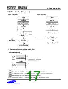
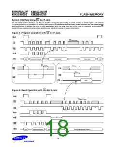
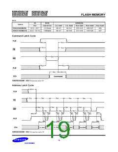
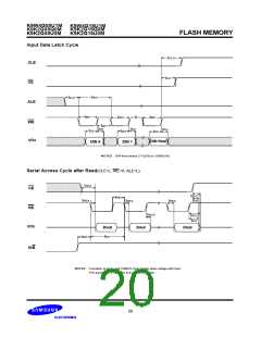
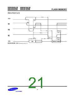
FLASH MEMORY
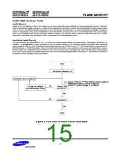
NAND Flash Technical Notes (Continued)
Erase Flow Chart
Read Flow Chart
Start
Write 00h
Start
Write 60h
Write Block Address
Write Address
Write 30h
Write D0h
Read Data
Read Status Register
ECC Generation
No
I/O 6 = 1 ?
or R/B = 1 ?
No
Verify ECC
Reclaim the Error
Yes
*
No
Yes
Erase Error
I/O 0 = 0 ?
Page Read Completed
Yes
Erase Completed
: If erase operation results in an error, map out
the failing block and replace it with another block.
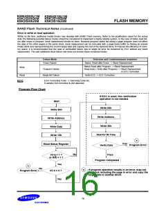
*
Block Replacement
Block A
1st
2
{
(n-1)th
nth
an error occurs.
(page)
Buffer memory of the controller.
Block B
1st
1
{
(n-1)th
nth
(page)
* Step1
When an error happens in the nth page of the Block ’A’ during erase or program operation.
* Step2
Copy the nth page data of the Block ’A’ in the buffer memory to the nth page of another free block. (Block ’B’)
* Step3
Then, copy the data in the 1st ~ (n-1)th page to the same location of the Block ’B’.
* Step4
Do not erase or program to Block ’A’ by creating an ’invalid Block’ table or other appropriate scheme.
17

 SAMSUNG [ SAMSUNG ]