K9F5608U0B-VCB0,VIB0,FCB0,FIB0
K9F5608Q0B-DCB0,DIB0,HCB0,HIB0
K9F5608U0B-YCB0,YIB0,PCB0,PIB0
K9F5608U0B-DCB0,DIB0,HCB0,HIB0
K9F5616Q0B-DCB0,DIB0,HCB0,HIB0
K9F5616U0B-YCB0,YIB0,PCB0,PIB0
K9F5616U0B-DCB0,DIB0,HCB0,HIB0
FLASH MEMORY
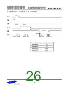
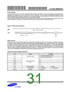
READ ID
The device contains a product identification mode, initiated by writing 90h to the command register, followed by an address input of
00h. Two read cycles sequentially output the manufacture code(ECh), and the device code respectively. The command register
remains in Read ID mode until further commands are issued to it. Figure 13 shows the operation sequence.
Figure 13. Read ID Operation
CLE
tCEA
CE
WE
tAR
ALE
RE
tWHR
tREA
Device
Code*
I/Ox
ECh
00h
90h
Address. 1cycle
Maker code
Device code
Device
Device Code*
K9F5608Q0B
K9F5608U0B
K9F5616Q0B
K9F5616U0B
35h
75h
45h
55h
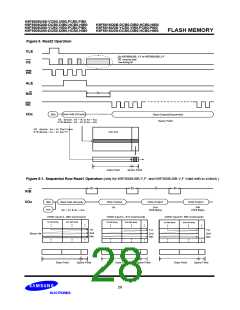
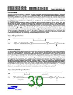
RESET
The device offers a reset feature, executed by writing FFh to the command register. When the device is in Busy state during random
read, program or erase mode, the reset operation will abort these operations. The contents of memory cells being altered are no
longer valid, as the data will be partially programmed or erased. The command register is cleared to wait for the next command, and
the Status Register is cleared to value C0h when WP is high. Refer to table 5 for device status after reset operation. If the device is
already in reset state a new reset command will not be accepted by the command register. The R/B pin transitions to low for tRST
after the Reset command is written. Refer to Figure 14 below.
Figure 14. RESET Operation
tRST
R/B
I/Ox
FFh
Table5. Device Status
After Power-up
After Reset
Operation Mode
Read 1
Waiting for next command
32

 SAMSUNG [ SAMSUNG ]