K9F5608U0B-VCB0,VIB0,FCB0,FIB0
K9F5608Q0B-DCB0,DIB0,HCB0,HIB0
K9F5608U0B-YCB0,YIB0,PCB0,PIB0
K9F5608U0B-DCB0,DIB0,HCB0,HIB0
K9F5616Q0B-DCB0,DIB0,HCB0,HIB0
K9F5616U0B-YCB0,YIB0,PCB0,PIB0
K9F5616U0B-DCB0,DIB0,HCB0,HIB0
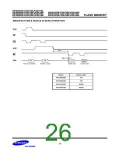
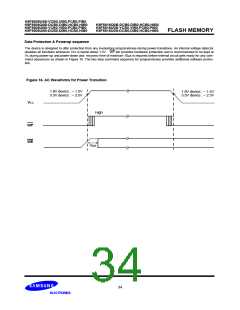
FLASH MEMORY
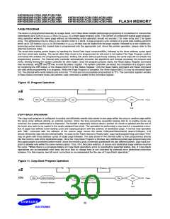
PAGE PROGRAM
The device is programmed basically on a page basis, but it does allow multiple partial page programing of a byte/word or consecutive
bytes/words up to 528(X8 device) or 264(X16 device), in a single page program cycle. The number of consecutive partial page program-
ming operation within the same page without an intervening erase operation should not exceed 2 for main array and 3 for spare
array. The addressing may be done in any random order in a block. A page program cycle consists of a serial data loading period in
which up to 528 bytes(X8 device) or 264 words(X16 device) of data may be loaded into the page register, followed by a non-volatile pro-
gramming period where the loaded data is programmed into the appropriate cell. About the pointer operation, please refer to the
attached technical notes.
The serial data loading period begins by inputting the Serial Data Input command(80h), followed by the three address cycles input
and then serial data loading. The words other than those to be programmed do not need to be loaded.The Page Program confirm
command(10h) initiates the programming process. Writing 10h alone without previously entering the serial data will not initiate the
programming process. The internal write controller automatically executes the algorithms and timings necessary for program and
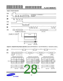
verify, thereby freeing the system controller for other tasks. Once the program process starts, the Read Status Register command
may be entered, with RE and CE low, to read the status register. The system controller can detect the completion of a program cycle
by monitoring the R/B output, or the Status bit(I/O 6) of the Status Register. Only the Read Status command and Reset command
are valid while programming is in progress. When the Page Program is complete, the Write Status Bit(I/O 0) may be checked(Figure
10). The internal write verify detects only errors for "1"s that are not successfully programmed to "0"s. The command register remains
in Read Status command mode until another valid command is written to the command register.
Figure 10. Program Operation
tPROG
R/B
I/Ox
Pass
80h
Address & Data Input
I/O0
Fail
10h
70h
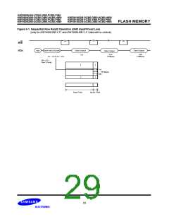
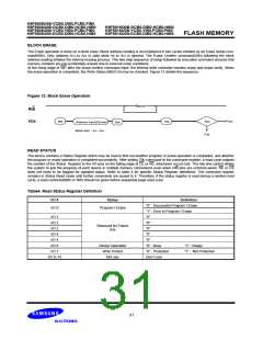
COPY-BACK PROGRAM
The copy-back program is configured to quickly and efficiently rewrite data stored in one page within the array to another page within
the same array without utilizing an external memory. Since the time-consuming sequently-reading and its re-loading cycles are
removed, the system performance is improved. The benefit is especially obvious when a portion of a block is updated and the rest of
the block also need to be copied to the newly assigned free block. The operation for performing a copy-back is a sequential execu-
tion of page-read without burst-reading cycle and copying-program with the address of destination page. A normal read operation
with "00h" command with the address of the source page moves the whole 528bytes/264words(X8 device:528bytes, X16
device:264words) data into the internal buffer. As soon as the Flash returns to Ready state, copy-back programming command "8Ah"
may be given with three address cycles of target page followed. The data stored in the internal buffer is then programmed directly
into the memory cells of the destination page. Once the Copy-Back Program is finished, any additional partial page programming into
the copied pages is prohibited before erase. Since the memory array is internally partitioned into two different planes, copy-back pro-
gram is allowed only within the same memory plane. Thus, A14, the plane address, of source and destination page address must be
the same. "When there is a program-failure at Copy-Back operation, error is reported by pass/fail status. But, if Copy-Back
operations are accumulated over time, bit error due to charge loss is not checked by external error detection/correction
scheme. For this reason, two bit error correction is recommended for the use of Copy-Back operation."
Figure 11. Copy-Back Program Operation
tR
tPROG
R/B
I/Ox
Add.(3Cycles)
Pass
Add.(3Cycles)
00h
I/O0
Fail
8Ah
70h
Source Address
Destination Address
30

 SAMSUNG [ SAMSUNG ]