K9F5608U0B-VCB0,VIB0,FCB0,FIB0
K9F5608Q0B-DCB0,DIB0,HCB0,HIB0
K9F5608U0B-YCB0,YIB0,PCB0,PIB0
K9F5608U0B-DCB0,DIB0,HCB0,HIB0
K9F5616Q0B-DCB0,DIB0,HCB0,HIB0
K9F5616U0B-YCB0,YIB0,PCB0,PIB0
K9F5616U0B-DCB0,DIB0,HCB0,HIB0
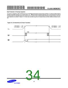
FLASH MEMORY
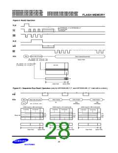
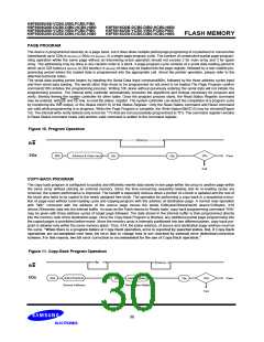
BLOCK ERASE
The Erase operation is done on a block basis. Block address loading is accomplished in two cycles initiated by an Erase Setup com-
mand(60h). Only address A14 to A24 is valid while A9 to A13 is ignored. The Erase Confirm command(D0h) following the block
address loading initiates the internal erasing process. This two-step sequence of setup followed by execution command ensures that
memory contents are not accidentally erased due to external noise conditions.
At the rising edge of WE after the erase confirm command input, the internal write controller handles erase and erase-verify. When
the erase operation is completed, the Write Status Bit(I/O 0) may be checked. Figure 12 details the sequence.
Figure 12. Block Erase Operation
tBERS
R/B
Pass
I/Ox
60h
I/O0
Fail
70h
Address Input(2Cycle)
Block Add. : A9 ~ A24
D0h
READ STATUS
The device contains a Status Register which may be read to find out whether program or erase operation is completed, and whether
the program or erase operation is completed successfully. After writing 70h command to the command register, a read cycle outputs
the content of the Status Register to the I/O pins on the falling edge of CE or RE, whichever occurs last. This two line control allows
the system to poll the progress of each device in multiple memory connections even when R/B pins are common-wired. RE or CE
does not need to be toggled for updated status. Refer to table 4 for specific Status Register definitions. The command register
remains in Status Read mode until further commands are issued to it. Therefore, if the status register is read during a random read
cycle, a read command(00h or 50h) should be given before sequential page read cycle.
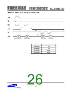
Table4. Read Status Register Definition
I/O #
Status
Definition
"0" : Successful Program / Erase
I/O 0
Program / Erase
"1" : Error in Program / Erase
I/O 1
I/O 2
"0"
"0"
"0"
"0"
"0"
Reserved for Future
Use
I/O 3
I/O 4
I/O 5
I/O 6
Device Operation
Write Protect
Not use
"0" : Busy
"1" : Ready
"1" : Not Protected
I/O 7
"0" : Protected
Don’t care
I/O 8~15
31

 SAMSUNG [ SAMSUNG ]