K9F5608U0B-VCB0,VIB0,FCB0,FIB0
K9F5608Q0B-DCB0,DIB0,HCB0,HIB0
K9F5608U0B-YCB0,YIB0,PCB0,PIB0
K9F5608U0B-DCB0,DIB0,HCB0,HIB0
K9F5616Q0B-DCB0,DIB0,HCB0,HIB0
K9F5616U0B-YCB0,YIB0,PCB0,PIB0
K9F5616U0B-DCB0,DIB0,HCB0,HIB0
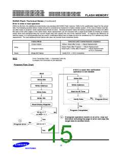
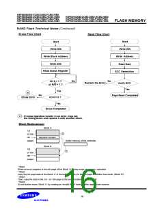
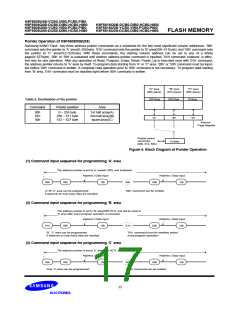
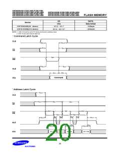
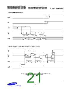
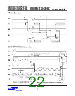
FLASH MEMORY
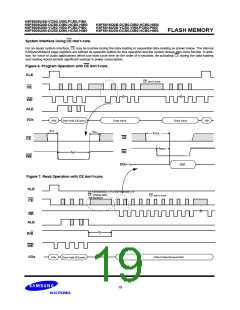
System Interface Using CE don’t-care.
For an easier system interface, CE may be inactive during the data-loading or sequential data-reading as shown below. The internal
528byte/264word page registers are utilized as seperate buffers for this operation and the system design gets more flexible. In addi-
tion, for voice or audio applications which use slow cycle time on the order of u-seconds, de-activating CE during the data-loading
and reading would provide significant savings in power consumption.
Figure 6. Program Operation with CE don’t-care.
CLE
CE don’t-care
CE
WE
ALE
I/Ox
80h
Start Add.(3Cycle)
Data Input
Data Input
10h
tCS
tCH
tCEA
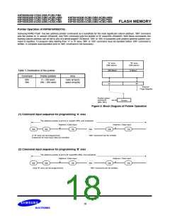
CE
RE
CE
tREA
tWP
WE
I/O0~15
out
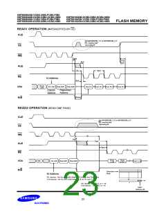
Figure 7. Read Operation with CE don’t-care.
CLE
On K9F5608U0B_Y,P or K9F5608U0B_V,F
CE must be held
low during tR
CE don’t-care
CE
RE
ALE
tR
R/B
WE
I/Ox
Data Output(sequential)
00h
Start Add.(3Cycle)
19

 SAMSUNG [ SAMSUNG ]