K9F2808U0B-YCB0,YIB0
K9F2808Q0B-DCB0,DIB0
K9F2808U0B-VCB0,VIB0 K9F2808U0B-DCB0,DIB0
FLASH MEMORY
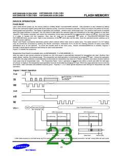
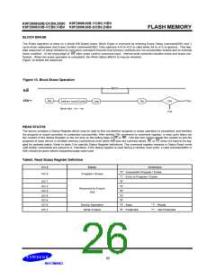
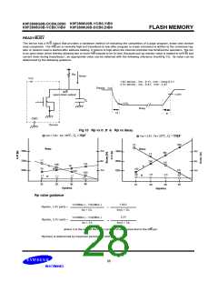
READY/BUSY
The device has a R/B output that provides a hardware method of indicating the completion of a page program, erase and random
read completion. The R/B pin is normally high but transitions to low after program or erase command is written to the command reg-
ister or random read is started after address loading. It returns to high when the internal controller has finished the operation. The pin
is an open-drain driver thereby allowing two or more R/B outputs to be Or-tied. Because pull-up resistor value is related to tr(R/B) and
current drain during busy(ibusy) , an appropriate value can be obtained with the following reference chart(Fig 13). Its value can be
determined by the following guidance.
Rp
ibusy
VCC
1.8V device - VOL : 0.1V, VOH : VCCq-0.1V
3.3V device - VOL : 0.4V, VOH : 2.4V
Ready Vcc
R/B
open drain output
VOH
CL
VOL
Busy
tf
tr
GND
Device
Fig 13 Rp vs tr ,tf & Rp vs ibusy
@ Vcc = 1.8V, Ta = 25
°
C , C = 30pF
@ Vcc = 3.3V, Ta = 25
°
C , C = 100pF
L
L
400
2.4
Ibusy
Ibusy
300n
3m
300n
3m
300
1.2
1.7
200n
100n
2m
1m
200n
100n
200
2m
1m
0.8
120
0.43
0.85
60
90
tr
tf
tr
30
100
3.6
0.6
0.57
3.6
2K
3.6
3K
3.6
tf
1.7
1.7
1.7
2K
1.7
4K
1K
3K
Rp(ohm)
4K
1K
Rp(ohm)
Rp value guidance
VCC(Max.) - VOL(Max.)
1.85V
Rp(min, 1.8V part) =
=
=
IOL + SIL
3mA + SIL
3.2V
VCC(Max.) - VOL(Max.)
Rp(min, 3.3V part) =
IOL + SIL
8mA + SIL
where IL is the sum of the input currents of all devices tied to the R/B pin.
Rp(max) is determined by maximum permissible limit of tr
28

 SAMSUNG [ SAMSUNG ]