K9F2808U0B-YCB0,YIB0
K9F2808Q0B-DCB0,DIB0
K9F2808U0B-VCB0,VIB0 K9F2808U0B-DCB0,DIB0
FLASH MEMORY
DEVICE OPERATION
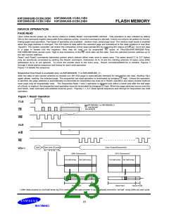
PAGE READ
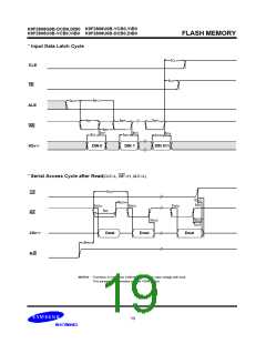
Upon initial device power up, the device status is initially Read1 command(00h) latched. This operation is also initiated by writing
00h to the command register along with three address cycles. Once the command is latched, it does not need to be written for the fol-
lowing page read operation. Two types of operation are available : random read, serial page read. The random read mode is enabled
when the page address is changed. The 528 bytes of data within the selected page are transferred to the data registers in less than
10ms(tR). The system controller can detect the completion of this data transfer(tR) by analyzing the output of R/B pin. Once the data
in
a page is loaded into the registers, they may be read out by sequential RE pulse of 70ns/50n(K9F2808Q0B:70ns,
K9F2808U0B:50ns) period cycle. High to low transitions of the RE clock take out the data from the selected column address up to
the last column address.
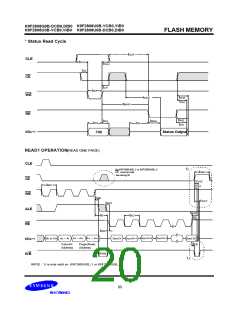
Read1 and Read2 commands determine pointer which selects either main area or spare area. The spare area(512 to 527 bytes)
may be selectively accessed by writing the Read2 command. Addresses A0 to A3 set the starting address of spare area while
addresses A4 to A7 are ignored. To move the pointer back to the main area, Read1 command(00h/01h) is needed. Figures 7
through 8 show typical sequence and timing for each read operation.
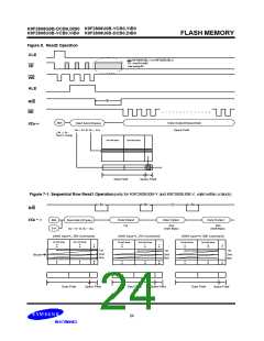
Figure 7,8 details the sequence.
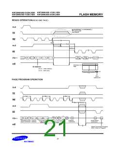
Sequential Row Read is available only on K9F2808U0B_Y or K9F2808U0B_V :
After the data of last column address is clocked out, the next page is automatically selected for sequential row read. Waiting 10ms
again allows reading the selected page. The sequential row read operation is terminated by bringing CE high. Unless the operation
is aborted, the page address is automatically incremented for sequential row read as in Read1 operation and spare sixteen bytesof
each page may be sequentially read. The Sequential Read 1 and 2 operation is allowed only within a block and after the last page
of a block is readout, the sequential read operation must be terminated by bringing CE high. When the page address moves onto the
next block, read command and address must be given. Figures 7-1, 8-1 show typical sequence and timings for sequential row read
operation.
Figure 7. Read1 Operation
CLE
On K9F2808U0B_Y or K9F2808U0B_V
CE must be held
low during tR
CE
WE
ALE
tR
R/B
RE
Start Add.(3Cycle)
A0 ~ A7 & A9 ~ A23
Data Output(Sequential)
(01h Command)*
00h
I/O0~7
(00h Command)
1st half array
2st half array
1st half array 2st half array
Data Field
Spare Field
Data Field
Spare Field
* After data access on 2nd half array by 01h command, the start pointer is automatically moved to 1st half array (00h) at next cycle.
23

 SAMSUNG [ SAMSUNG ]