K9F2808U0B-YCB0,YIB0
K9F2808Q0B-DCB0,DIB0
K9F2808U0B-VCB0,VIB0 K9F2808U0B-DCB0,DIB0
FLASH MEMORY
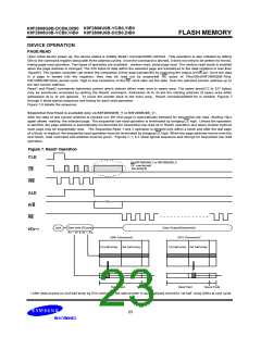
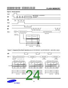
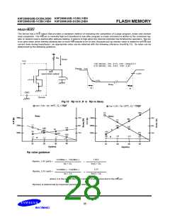
Figure 8. Read2 Operation
CLE
On K9F2808U0B_Y or K9F2808U0B_V
CE must be held
low during tR
CE
WE
ALE
tR
R/B
RE
50h
Data Output(Sequential)
Spare Field
Start Add.(3Cycle)
A0 ~ A3 & A9 ~ A23
I/O0~7
(A4 ~ A7 :
Don¢t Care)
1st half array
2nd half array
Data Field
Spare Field
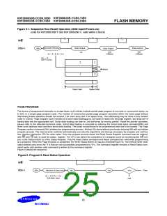
Figure 7-1. Sequential Row Read1 Operation(only for K9F2808U0B-Y and K9F2808U0B-V, valid within a block)
tR
tR
tR
R/B
Data Output
1st
Data Output
Data Output
I/O0 ~ 7
00h
01h
Start Add.(3Cycle)
A0 ~ A7 & A9 ~ A24
2nd
(528 Byte)
Nth
(528 Byte)
(GND input=L, 00h Command)
(GND input=L, 01h Command)
(GND input=H, 00h Command)
1st half array
2nd half array
1st half array
2nd half array
1st half array
2nd half array
1st
1st
2nd
Nth
1st
2nd
Nth
2nd
Nth
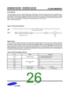
Block
Data Field
Spare Field
Data Field
Spare Field
Data Field
Spare Field
24

 SAMSUNG [ SAMSUNG ]