256M GDDR3 SDRAM
K4J55323QG
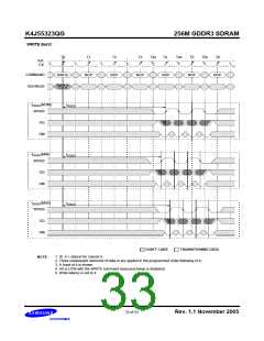
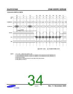
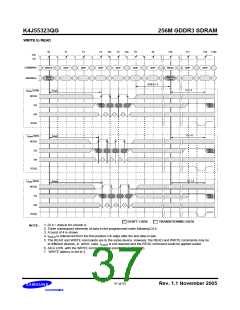
WRITE to READ
T0
T1
T2
T3
T3n
T4
T4n
T5
T6
T10
T17
T18
T18n
/CK
CK
COMMAND
ADDRESS
WRITE
NOP
NOP
NOP
NOP
NOP
NOP
READ
NOP
NOP
Bank
Col b
Bank a.
Col n
tCDLR = 5
t
CL = 8
t
(NOM)
DQSS
DQSS
DQSS
DQSS
WDQS
DI
b
DI
n
DQ
DM
RDQS
CL = 8
t
t
(MIN)
DQSS
WDQS
DI
DI
n
DQ
b
DM
RDQS
t
CL = 8
t
(MAX)
DQSS
WDQS
DI
b
DI
n
DQ
DM
RDQS
DON’T CARE
TRANSITIONING DATA
1. DI b = data-in for column b.
NOTE :
2. Three subsequent elements of data-in the programmed order following DI b.
3. A burst of 4 is shown.
4. tCDLR is referenced from the first positive CK edge after the last data-in pair.
5. The READ and WRITE commands are to the same device. However, the READ and WRITE commands may be
to different devices, in which case tCDLR is not required and the READ command could be applied earlier.
6. A8 is LOW with the WRITE command (auto precharge is disabled).
7. WRITE latency is set to 3
37 of 53
Rev. 1.1 November 2005

 SAMSUNG [ SAMSUNG ]