DDR SDRAM 256Mb E-die (x4, x8)
DDR SDRAM
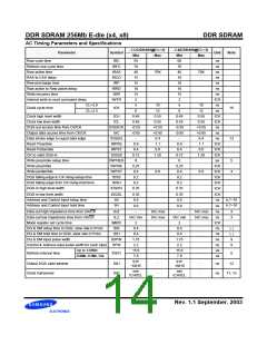
- CC(DDR400@CL=3)
- C4(DDR400@CL=3)
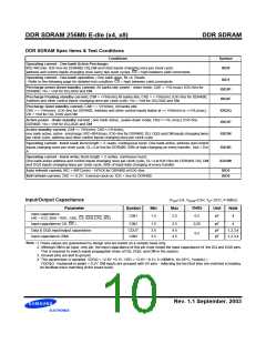
Parameter
Data hold skew factor
Symbol
Unit
Note
Min
Max
0.5
-
Min
Max
0.5
-
tQHS
tDAL
ns
ns
12
14
15
Auto Precharge write recovery + precharge time
Exit self refresh to non-READ command
Exit self refresh to READ command
-
-
tXSNR
tXSRD
75
75
ns
200
-
200
-
tCK
Component Notes
1.VID is the magnitude of the difference between the input level on CK and the input level on CK.
2. The value of VIX is expected to equal 0.5*VDDQ of the transmitting device and must track variations in the dc level of the same.
3. tHZ and tLZ transitions occur in the same access time windows as valid data transitions. these parameters are not referenced to a
specific voltage level but specify when the device output in no longer driving (HZ), or begins driving (LZ).
4. The maximum limit for this parameter is not a device limit. The device will operate with a greater value for this parameter, but sys
tem performance (bus turnaround) will degrade accordingly.
5. The specific requirement is that DQS be valid (HIGH, LOW, or at some point on a valid transition) on or before this CK edge. A
valid transition is defined as monotonic and meeting the input slew rate specifications of the device. when no writes were previ
ously in progress on the bus, DQS will be tran sitioning from High- Z to logic LOW. If a previous write was in progress, DQS could
be HIGH, LOW, or transitioning from HIGH to LOW at this time, depending on tDQSS.
6. A maximum of eight AUTO REFRESH commands can be posted to any given DDR SDRAM device.
7. For command/address input slew rate ≥ 0.5 V/ns
8. For CK & CK slew rate ≥ 0.5 V/ns
9. These parameters guarantee device timing, but they are not necessarily tested on each device. They may be guaranteed by
device design or tester correlation.
10. Slew Rate is measured between VOH(ac) and VOL(ac).
11. Min (tCL, tCH) refers to the smaller of the actual clock low time and the actual clock high time as provided to the device (i.e. this
value can be greater than the minimum specification limits for tCL and tCH).....For example, tCL and tCH are = 50% of the
period, less the half period jitter (tJIT(HP)) of the clock source, and less the half period jitter due to crosstalk (tJIT(crosstalk)) into
the clock traces.
12. tQH = tHP - tQHS, where:
tHP = minimum half clock period for any given cycle and is defined by clock high or clock low (tCH, tCL). tQHS accounts for 1) The
pulse duration distortion of on-chip clock circuits; and 2) The worst case push-out of DQS on one tansition followed by the worst
case pull-in of DQ on the next transition, both of which are, separately, due to data pin skew and output pattern effects, and p-
channel to n-channel variation of the output drivers.
13. tDQSQ
Consists of data pin skew and output pattern effects, and p-channel to n-channel variation of the output drivers for any given
cycle.
14. tDAL = (tWR/tCK) + (tRP/tCK)
For each of the terms above, if not already an integer, round to the next highest integer. Example: For DDR400(CC) at CL=3 and
tCK=5ns tDAL = (15 ns / 5 ns) + (15 ns/ 5ns) = {(3) + (3)}CLK
tDAL = 6 clocks
15. In all circumstances, tXSNR can be satisfied using tXSNR=tRFCmin+1*tCK
16. The only time that the clock frequency is allowed to change is during self-refresh mode.
Rev. 1.1 September. 2003

 SAMSUNG [ SAMSUNG ]