DDR SDRAM 256Mb E-die (x4, x8)
DDR SDRAM
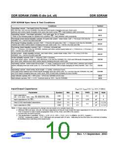
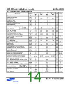
AC Timing Parameters and Specifications
- CC(DDR400@CL=3)
- C4(DDR400@CL=3)
Parameter
Symbol
Unit
Note
Min
55
Max
Min
60
Max
Row cycle time
tRC
tRFC
tRAS
tRCD
tRP
ns
ns
Refresh row cycle time
Row active time
70
70
40
70K
40
70K
ns
RAS to CAS delay
15
18
ns
Row precharge time
15
18
ns
Row active to Row active delay
Write recovery time
tRRD
tWR
10
10
ns
15
15
ns
Internal write to read command delay
tWTR
2
2
tCK
ns
CL=3.0
CL=2.5
5
10
12
5
10
12
Clock cycle time
tCK
16
13
6
6
ns
Clock high level width
Clock low level width
tCH
tCL
0.45
0.45
-0.55
-0.65
-
0.55
0.55
+0.55
+0.65
0.4
0.45
0.45
-0.55
-0.65
-
0.55
0.55
+0.55
+0.65
0.4
tCK
tCK
ns
DQS-out access time from CK/CK
Output data access time from CK/CK
Data strobe edge to ouput data edge
Read Preamble
tDQSCK
tAC
ns
tDQSQ
tRPRE
tRPST
tDQSS
tWPRES
tWPRE
tWPST
tDSS
ns
0.9
0.4
0.72
0
1.1
0.9
0.4
0.72
0
1.1
tCK
tCK
tCK
ps
Read Postamble
0.6
0.6
CK to valid DQS-in
1.28
1.28
Write preamble setup time
Write preamble
5
4
0.25
0.4
0.2
0.2
0.35
0.25
0.4
0.2
0.2
0.35
tCK
tCK
tCK
tCK
tCK
tCK
ns
Write postamble
0.6
0.6
DQS falling edge to CK rising-setup time
DQS falling edge from CK rising-hold time
DQS-in high level width
tDSH
tDQSH
DQS-in low level width
tDQSL
tIS
0.35
0.6
0.35
0.6
Address and Control Input setup time
Address and Control Input hold time
h,7~10
h,7~10
tIH
0.6
0.6
ns
Data-out high impedence time from CK/CK
Data-out low impedence time from CK/CK
Mode register set cycle time
tHZ
tLZ
-
tAC max
tAC max
-
tAC max
tAC max
ns
3
3
tAC min
2
tAC min
2
ns
tMRD
tDS
tCK
ns
DQ & DM setup time to DQS, slew rate 0.5V/ns
DQ & DM hold time to DQS, slew rate 0.5V/ns
DQ & DM input pulse width
0.4
0.4
i, j
i, j
9
tDH
0.4
0.4
ns
tDIPW
tIPW
1.75
2.2
1.75
2.2
ns
Control & Address input pulse width for each input
ns
9
Up to 128Mb
Refresh interval time
15.6
7.8
15.6
7.8
us
tREFI
6
256Mb, 512Mb, 1Gb
us
tHP
-tQHS
tHP
-tQHS
Output DQS valid window
Clock half period
tQH
tHP
-
-
-
-
ns
ns
12
min
tCH/tCL
min
tCH/tCL
11, 12
Rev. 1.1 September. 2003

 SAMSUNG [ SAMSUNG ]