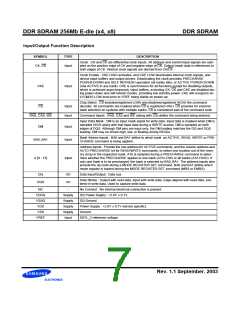
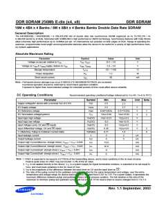
DDR SDRAM 256Mb E-die (x4, x8)
DDR SDRAM
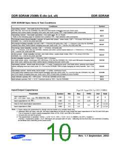
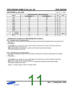
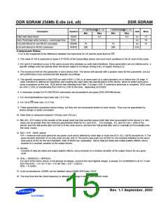
DDR SDRAM I spec table
(VDD=2.7V, T = 10°C)
DD
64Mx4 (K4H560438E), 32Mx8 (K4H560838E)
CC(DDR400@CL=3) C4(DDR400@CL=3)
105 100
Symbol
Unit
Notes
IDD0
IDD1
mA
mA
mA
mA
mA
mA
mA
mA
mA
mA
mA
mA
mA
130
4
130
4
IDD2P
IDD2F
IDD2Q
IDD3P
IDD3N
IDD4R
IDD4W
IDD5
30
30
25
25
55
55
75
75
185
190
180
3
185
190
180
3
Normal
IDD6
Low power
Optional
1.5
310
1.5
290
IDD7A
< Detailed test conditions for DDR SDRAM IDD1 & IDD7A >
IDD1 : Operating current: One bank operation
1. Only one bank is accessed with tRC(min), Burst Mode, Address and Control inputs change logic state once per Deselect cycle.
Iout = 0mA
2. Timing patterns
- CC/C4(200Mhz,CL=3) : tCK=5ns, CL=3, BL=4, tRCD=3*tCK(CC) 4*tCK(C4), tRC=11*tCK(CC) 12*tCK(C4), tRAS=8*tCK
Setup : A0 N N R0 N N N N P0 N N
Read : A0 N N R0 N N N N P0 N N - repeat the same timing with random address changing
*50% of data changing at every transfer
IDD7A : Operating current: Four bank operation
1. Four banks are being interleaved with tRC(min), Burst Mode, Address and Control inputs on Deselet edge are not changing.
Iout = 1mA
2. Timing patterns
- CC/C4(200Mhz,CL=3) : tCK=5ns, CL=3, BL=4, tRCD=3*tCK(CC) 4*tCK(C4), tRC=11*tCK(CC) 12*tCK(C4), tRAS=8*tCK
Setup : A0 N A1 RA0 A2 RA1 A3 RA2 N RA3 N N
Read : A0 N A1 RA0 A2 RA1 A3 RA2 N RA3 N N - repeat the same timing with random address changing
*50% of data changing at every transfer
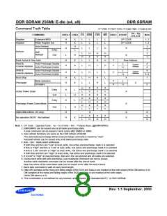
Legend : A = Activate, R=Read, W=Write, P=Precharge, N=NOP
Rev. 1.1 September. 2003

 SAMSUNG [ SAMSUNG ]