DDR SDRAM 256Mb E-die (x4, x8)
DDR SDRAM
16M x 4Bit x 4 Banks / 8M x 8Bit x 4 Banks Banks Double Data Rate SDRAM
General Description
The K4H560438E / K4H560838E / is 268,435,456 bits of double data rate synchronous DRAM organized as 4x 16,785,216 / 4x
8,388,608 words by 4/ 8bits, fabricated with SAMSUNG′s high performance CMOS technology. Synchronous features with Data Strobe
allow extremely high performance up to 333Mb/s per pin. I/O transactions are possible on both edges of DQS. Range of operating fre-
quencies, programmable burst length and programmable latencies allow the device to be useful for a variety of high performance mem-
ory system applications.
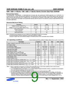
Absolute Maximum Rating
Parameter
Symbol
Value
Unit
Voltage on any pin relative to VSS
VIN, VOUT
-0.5 ~ 3.6
V
Voltage on VDD & VDDQ supply relative to VSS
Storage temperature
VDD, VDDQ
TSTG
PD
-1.0 ~ 3.6
-55 ~ +150
1.5
V
°C
W
Power dissipation
Short circuit current
IOS
50
mA
Note : Permanent device damage may occur if ABSOLUTE MAXIMUM RATINGS are exceeded.
Functional operation should be restricted to recommend operation condition.
Exposure to higher than recommended voltage for extended periods of time could affect device reliability.
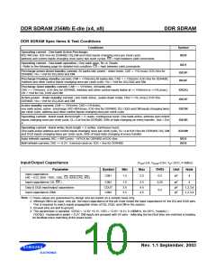
DC Operating Conditions
Recommended operating conditions(Voltage referenced to VSS=0V, TA=0 to 70°C)
Parameter
Symbol
Min
Max
2.7
Unit
Note
Supply voltage(for device with a nominal VDD of 2.5V)
VDD
2.5
I/O Supply voltage
VDDQ
VREF
VTT
2.5
2.7
V
V
I/O Reference voltage
I/O Termination voltage(system)
0.49*VDDQ
VREF-0.04
0.51*VDDQ
VREF+0.04
1
2
V
Input logic high voltage
VIH(DC)
VIL(DC)
VIN(DC)
VID(DC)
VI(Ratio)
II
VREF+0.15
-0.3
VDDQ+0.3
VREF-0.15
VDDQ+0.3
VDDQ+0.6
1.4
V
Input logic low voltage
V
Input Voltage Level, CK and CK inputs
Input Differential Voltage, CK and CK inputs
V-I Matching: Pullup to Pulldown Current Ratio
Input leakage current
-0.3
V
0.36
0.71
-2
V
3
4
-
2
uA
uA
mA
Output leakage current
IOZ
-5
5
Output High Current(Normal strengh driver) ;VOUT = VTT + 0.84V
IOH
-16.8
Output High Current(Normal strengh driver) ;VOUT = VTT - 0.84V
Output High Current(Half strengh driver) ;VOUT = VTT + 0.45V
Output High Current(Half strengh driver) ;VOUT = VTT - 0.45V
IOL
IOH
IOL
16.8
-9
mA
mA
mA
9
Note :
1.VREF is expected to be equal to 0.5*VDDQ of the transmitting device, and to track variations in the dc level of same.
Peak-to peak noise on VREF may not exceed +/-2% of the dc value.
2. VTT is not applied directly to the device. VTT is a system supply for signal termination resistors, is expected to be set equal to
VREF, and must track variations in the DC level of VREF
3. VID is the magnitude of the difference between the input level on CK and the input level on CK.
4. The ratio of the pullup current to the pulldown current is specified for the same temperature and voltage, over the entire
temperature and voltage range, for device drain to source voltages from 0.25V to 1.0V. For a given output, it represents the
maximum difference between pullup and pulldown drivers due to process variation. The full variation in the ratio of the
maximum to minimum pullup and pulldown current will not exceed 1/7 for device drain to source voltages from 0.1 to 1.0.
Rev. 1.1 September. 2003

 SAMSUNG [ SAMSUNG ]