Rev. 1.01
K4B2G0446D
K4B2G0846D
datasheet
DDR3L SDRAM
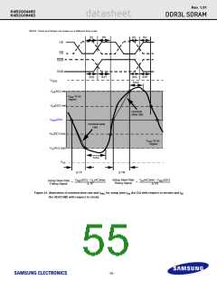
14.4 Data Setup, Hold and Slew Rate Derating :
For all input signals the total tDS (setup time) and tDH (hold time) required is calculated by adding the data sheet tDS(base) and tDH(base) value (see
Table 54) to the ∆ tDS and ∆tDH (see Table 55) derating value respectively. Example: tDS (total setup time) = tDS(base) + ∆tDS.
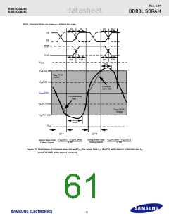
Setup (tDS) nominal slew rate for a rising signal is defined as the slew rate between the last crossing of VREF(DC) and the first crossing of VIH(AC)min.
Setup (tDS) nominal slew rate for a falling signal is defined as the slew rate between the last crossing of VREF(DC) and the first crossing of VIL(AC)max
(see Figure 25). If the actual signal is always earlier than the nominal slew rate line between shaded ’VREF(DC) to ac region’, use nominal slew rate for
derating value. If the actual signal is later than the nominal slew rate line anywhere
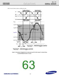
between shaded ’VREF(DC) to ac region’, the slew rate of a tangent line to the actual signal from the ac level to dc level is used for derating value (see
Figure 27).
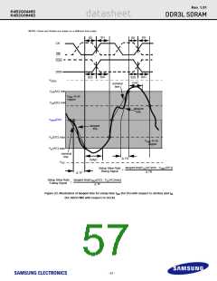
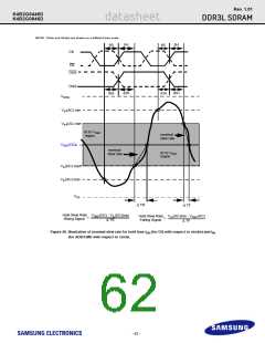
Hold (tDH) nominal slew rate for a rising signal is defined as the slew rate between the last crossing of VIL(DC)max and the first crossing of VREF(DC).
Hold (tDH) nominal slew rate for a falling signal is defined as the slew rate between the last crossing of VIH(DC)min and the first crossing of VREF(DC)
(see Figure ). If the actual signal is always later than the nominal slew rate line between shaded ’dc level to VREF(DC) region’, use nominal slew rate for
derating value. If the actual signal is earlier than the nominal slew rate line anywhere between shaded ’dc to VREF(DC) region’, the slew rate of a tangent
line to the actual signal from the dc level to VREF(DC) level is used for derating value (see Figure 28).
For a valid transition the input signal has to remain above/below VIH/IL(AC) for some time tVAC (see Table 56).
Although for slow slew rates the total setup time might be negative (i.e. a valid input signal will not have reached VIH/IL(AC) at the time of the rising clock
transition) a valid input signal is still required to complete the transition and reach VIH/IL(AC).
For slew rates in between the values listed in the tables the derating values may obtained by linear interpolation.
These values are typically not subject to production test. They are verified by design and characterization.
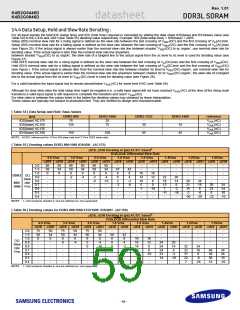
[ Table 54 ] Data Setup and Hold Base-Values
[ps]
DDR3-800
DDR3-1066
DDR3-1333
DDR3-1600
reference
VIH/L(AC)
VIH/L(AC)
VIH/L(AC)
VIH/L(DC)
tDS(base) AC175
tDS(base) AC150
tDS(base) AC135
tDH(base) DC100
75
125
-
25
75
-
-
-
30
-
65
10
-
45
150
100
NOTE : AC/DC referenced for 1V/ns DQ-slew rate and 2 V/ns DQS slew rate)
[ Table 55 ] Derating values DDR3-800/1066 tDS/tDH - (AC175)
∆tDS, ∆tDH Derating in [ps] AC/DC based1
DQS,DQS Differential Slew Rate
4.0 V/ns
3.0 V/ns
2.0 V/ns
1.8 V/ns
1.6 V/ns
1.4V/ns
1.2V/ns
1.0V/ns
∆tDS ∆tDH ∆tDS ∆tDH ∆tDS ∆tDH ∆tDS ∆tDH ∆tDS ∆tDH ∆tDS ∆tDH ∆tDS ∆tDH ∆tDS ∆tDH
2.0
1.5
1.0
0.9
0.8
0.7
0.6
0.5
0.4
88
59
0
-
50
34
0
-
88
59
0
-2
-
50
34
0
-4
-
88
59
0
-2
-6
-
-
-
50
34
0
-4
-10
-
-
-
-
67
8
6
2
-3
-
-
42
8
-
-
16
14
10
5
-1
-
-
-
-
-
-
-
-
-
-
-
-
-
-
-
-
-
-
16
12
6
-
-
-
-
DDR3 DQ
4
22
18
13
7
-11
-
20
14
8
-2
-16
-
-
-
-
-
-
-
-
Slew
-
-
-2
-8
-
-
-
26
21
15
-2
-30
24
18
8
-6
-26
800/ rate
1066 V/ns
-
-
-
-
0
29
23
6
34
24
10
-10
-
-
-
-
-
-
-10
-
-
-
-
-
-
-
-
-
-
-
-
-22
NOTE : 1. Cell contents shaded in red are defined as ’not supported’.
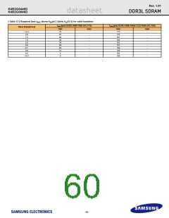
[ Table 56 ] Derating values for DDR3-800/1066/1333/1600 tDS/tDH - (AC150)
∆tDS, ∆tDH Derating in [ps] AC/DC based1
DQS,DQS Differential Slew Rate
4.0 V/ns
3.0 V/ns
2.0 V/ns
1.8 V/ns
1.6 V/ns
1.4V/ns
1.2V/ns
1.0V/ns
∆tDS ∆tDH ∆tDS ∆tDH ∆tDS ∆tDH ∆tDS ∆tDH ∆tDS ∆tDH ∆tDS ∆tDH ∆tDS ∆tDH ∆tDS ∆tDH
2.0
1.5
1.0
0.9
0.8
0.7
0.6
0.5
0.4
75
50
0
-
50
34
0
-
75
50
0
0
-
50
34
0
-4
-
75
50
0
0
0
-
50
34
0
-4
-10
-
-
-
-
58
8
8
8
8
-
-
42
8
-
-
-
-
-
-
-
-
-
-
-
-
-
-
-
-
-
16
16
16
16
15
-
16
12
6
-
-
-
-
-
DQ
Slew
rate
4
24
24
24
23
14
-
20
14
8
-2
-16
-
-
-
-
-
-
-
-
-
-2
-8
-
-
-
32
32
31
22
7
24
18
8
-6
-26
-
-
-
-
0
40
39
30
15
34
24
10
-10
V/ns
-
-
-
-
-
-
-
-10
-
-
-
-
-
-
-
-
-
-
-
-
-
-
NOTE : 1. Cell contents shaded in red are defined as ’not supported’.
- 59 -

 SAMSUNG [ SAMSUNG ]